



TSMC 2nm allocation is expanding after N2 entered high-volume manufacturing in Q4 2025. TSMC says demand is strong across smartphones and high-performance computing, but its public disclosures do not establish that Apple controls 100% of output, a fixed $30,000 wafer price, or a published monthly allocation by customer. The useful question is how a new-node ramp is allocated when yield, design risk, packaging and product economics all matter at once.
The “Apple locks out rivals” framing is attractive because it turns a complex supply chain into a clean headline. It is also too certain. In this analysis, confirmed means a company or regulator has disclosed it; illustrative means the number is a transparent scenario; and unverified means the public record does not support the claim. That distinction matters for procurement teams, investors and engineers who may reuse an article as a reference.
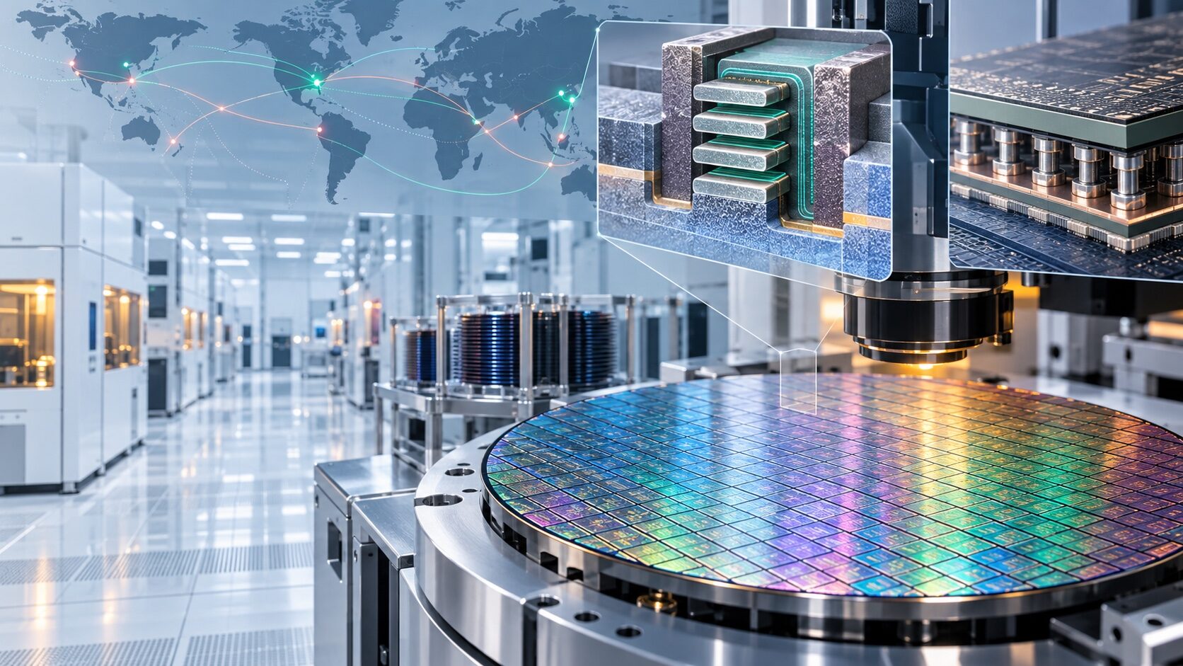
What TSMC has actually confirmed about N2
TSMC’s 2025 annual report says N2 entered high-volume manufacturing in the fourth quarter of 2025 with good yield and was expected to ramp quickly in 2026. The company also describes multiple N2 phases at Hsinchu and Kaohsiung and strong demand from smartphone and HPC applications in its first-quarter 2026 earnings transcript.
That evidence supports three conclusions: N2 is a commercial process, early supply is ramp constrained, and both mobile and HPC customers are relevant. It does not reveal the private split between customers. The TSMC smartphone technology page positions N2 as a nanosheet platform for smartphones and HPC, while N2P is presented as a later performance and power extension. Those are stronger anchors than anonymous allocation figures repeated across news and social posts.
Not established by a public primary source: Apple’s exact percentage of N2 capacity; exact customer wafer starts per month; a universal N2 wafer price; specific A-series or M-series die sizes; or a claim that NVIDIA, AMD, Qualcomm and MediaTek were “locked out.” Treat those statements as rumors until a company filing, earnings call or foundry disclosure supports them.
Why a new node creates an allocation problem
A leading-edge node is a coordinated manufacturing system, not a SKU that can be switched on for every customer at once. A foundry must qualify process recipes, design rules, standard cell libraries, SRAM, inspection, metrology and packaging interfaces. Customers must tape out designs, complete silicon validation and accept the risk of changing a product roadmap while the process is still learning.
The first allocation decision therefore weighs more than the price of a wafer. A customer with a very large product forecast can help absorb fixed engineering costs and provide predictable demand. A customer with a small die can produce more gross dies per wafer, while a large AI die may need advanced packaging and has a higher exposure to random defects. Those are economic reasons a customer mix may evolve during a ramp; they are not proof of an exclusive contract.
Nanosheets change the transistor architecture
TSMC describes N2 as a nanosheet transistor platform. In a FinFET, the gate controls three sides of a raised silicon fin. In a gate-all-around nanosheet design, the gate surrounds the channel, improving electrostatic control and allowing the process to tune sheet width. The manufacturing challenge is greater: the process must form and release stacked layers, control interfaces and keep variation within the design kit’s limits.
TSMC’s public N2 material cites a published target of higher speed at the same power, lower power at the same speed and increased chip density compared with its prior generation. Those figures are process-level claims under specified conditions, not a guaranteed uplift for every chip. Real product results depend on architecture, libraries, voltage, memory, thermal design and software.
TSMC N2, N2P and A16: do not collapse them into one node
The roadmap matters because “2nm” is a family label. TSMC’s annual report lists N2P and A16 as extensions, with volume production scheduled for the second half of 2026. TSMC describes A16 with Super Power Rail for HPC products that have complex signal routes and dense power delivery. That does not mean every N2 wafer has backside power delivery, nor that A16 is simply N2 with a smaller transistor.
| Platform | What the primary source says | Allocation implication |
|---|---|---|
| TSMC N2 | Nanosheet platform; HVM in Q4 2025; smartphone and HPC demand. | Early capacity must be qualified design by design. |
| N2P / A16 | Later extensions; A16 adds Super Power Rail for selected HPC use cases. | A later option can change the performance, power and packaging trade-off. |
| Intel 18A | Intel combines RibbonFET gate-all-around transistors with PowerVia backside power. | A credible alternative must be judged through PDK, yield, packaging and customer qualification. |
| Samsung SF2 | Samsung’s 2nm family uses its GAA/MBCFET roadmap and has separate HPC and automotive variants. | A second source can improve resilience, but node names are not directly comparable. |
The comparison uses each manufacturer’s own terminology. See Intel’s 18A process page and Samsung Foundry’s technology overview for the vendor-specific architecture descriptions. “2nm,” “18A” and “SF2” are marketing and generation labels; they are not a common measurement of physical gate length.
A transparent yield scenario: why die size changes the economics
The draft version of this article presented wafer prices, defect density and die areas as if they were disclosed product facts. They were not. The following is a reusable illustrative model so readers can see the mechanism without confusing assumptions with company data.
Assume a 300mm wafer priced at $30,000, defect density D0 of 0.08 defects/cm², and two hypothetical die areas: 100mm² and 600mm². Actual foundry prices, defect maps, redundancy, test yield, packaging yield and binning vary by process and design.
Using a Gross Dies Per Wafer estimate and the Murphy clustered-defect model, the 100mm² case produces about 640 gross dies, 92.36% modeled yield and 591 good dies, or roughly $50.76 of raw wafer cost per good die. The 600mm² case produces about 90 gross dies, 63.08% modeled yield and 56 good dies, or roughly $535.71 per good die. The difference is driven by area and the assumed defect density. It is not an estimate of an Apple, NVIDIA or AMD product.
import math

def murphy_yield(area_cm2, d0):
    ad = area_cm2 * d0
    return ((1 - math.exp(-ad)) / ad) ** 2 if ad else 1.0

def scenario(die_mm2, wafer_cost=30000, d0=0.08):
    wafer_area = math.pi * 150**2
    edge_loss = math.pi * 300 / math.sqrt(2 * die_mm2)
    gross = int(wafer_area / die_mm2 - edge_loss)
    y = murphy_yield(die_mm2 / 100, d0)
    good = int(gross * y)
    return gross, y, good, wafer_cost / good

for die in (100, 600):
    print(die, scenario(die))
What Apple’s early lead means—and what it does not
Apple has a long history of adopting TSMC’s advanced nodes early, and Apple’s own M6 announcement identifies M6 as Apple’s first 2nm chip. That is evidence of an early Apple product, not a disclosure of a 100% reservation. The most defensible description is that Apple appears well positioned to be an important early N2 customer while other customers qualify products against their own schedules.
For AI accelerators, the choice is multidimensional. A designer may prefer a mature node with better yield, a chiplet architecture that keeps individual dies smaller, or a later process with a stronger power-delivery option. That logic connects to the broader systems story covered in EyesTech’s analysis of H100 cloud pricing and datacenter economics and KV-cache and model architecture trade-offs. Silicon node leadership matters, but system throughput, memory, interconnect, cooling and utilization decide the customer’s economics.
Siddharth Roy’s allocation audit workflow
This article follows Siddharth Roy, EyesTech’s Global Tech Policy & Semiconductor Analyst, through a five-step review designed for claims that mix engineering, business and geopolitics.
- Classify the source: separate a filing, earnings transcript, product page, trade report and anonymous claim.
- Normalize the node: record the manufacturer, generation, power-delivery architecture, design kit and production window before comparing labels.
- Test capacity language: accept “multiple phases” or “strong demand” as qualitative evidence, while requiring a primary source for customer percentages and WSPM.
- Model unit economics: show wafer cost, die area, modeled yield and packaging as separate inputs so a reader can change the assumptions.
- Map policy risk: connect Taiwan concentration, export controls, packaging capacity and second-source qualification to the system’s real deployment timeline.
The same discipline is useful when evaluating supply risks in other technical markets, from 800V DC datacenter power to the operational limits of fiber-optic FPV systems. A strong technical article should show readers how to check the conclusion, not only tell them which conclusion to repeat.
A sourcing decision framework for 2026
- Choose N2 early when the product’s performance or power target justifies qualification cost and the team can absorb ramp uncertainty.
- Stay on a mature node when volume, yield and predictable packaging matter more than first access to a new transistor architecture.
- Use chiplets when partitioning can reduce large-die exposure and place I/O, analog and memory interfaces on the most economical process.
- Qualify a second foundry when resilience is worth the engineering cost; a slide deck claim of “dual sourcing” is not the same as a production-qualified backup.
The strategic takeaway is narrower and more useful than “Apple monopolized 2nm.” TSMC has moved N2 into high-volume manufacturing, the ramp is attracting both smartphone and HPC demand, and later N2-family options may change the power and packaging equation. Customer allocation remains partly private. Readers should treat exact percentages, prices, die sizes and rival roadmaps as claims requiring fresh evidence.
Frequently asked questions
Has TSMC N2 entered volume production?
Yes. TSMC’s 2025 annual report says N2 entered high-volume manufacturing in Q4 2025 with good yield and was ramping in 2026.
Did Apple secure 100% of TSMC’s 2nm capacity?
No public official disclosure reviewed for this article establishes that exact percentage. Apple is an early 2nm customer, but the customer split and contract terms are not publicly quantified.
Is TSMC N2 the same as Intel 18A or Samsung SF2?
No. All three use generation labels and advanced transistor terminology, but their design rules, libraries, power delivery, packaging and performance targets differ. Compare measured product data and qualification status rather than the label alone.
Why do large dies usually cost more per good die?
A larger die fits fewer times on a wafer and has a greater chance of intersecting a defect under the same modeled defect density. The scenario in this article demonstrates the mechanism; actual product cost also depends on redundancy, test, binning, packaging and contractual price.
Reviewed 15 September 2026 by Siddharth Roy, Global Tech Policy & Semiconductor Analyst, using TSMC, Apple, Intel and Samsung primary disclosures linked in context. Claims are labelled as confirmed, illustrative or unverified. EyesTech updates technical articles when a primary source changes and accepts corrections through its editorial policy.