
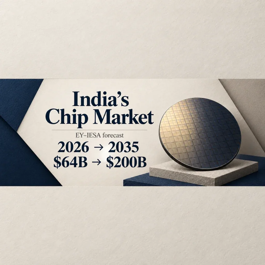

India’s semiconductor appetite is expanding at an unprecedented pace. Domestic consumption is projected to surge from $64 billion in 2026 to $200 billion by 2035, charting a rapid 12.2% compound annual growth rate (CAGR).
Between FY17 and FY25, direct semiconductor imports spiked from $5.7 billion to $30.3 billion. This fivefold surge was propelled by domestic electronics assembly plants that rapidly scaled finished device volumes, yet remained almost entirely dependent on imported silicon.
The landmark EY-IESA report, titled Semicon India 2.0: From Capacity Creation to Ecosystem Leadership, marks a critical turning point. Unveiled by the India Electronics and Semiconductor Association (IESA) at SEMICON India in New Delhi, it details the transition toward domestic manufacturing autonomy.
National policy has committed over ₹1.5 lakh crore ($18+ billion) in fiscal incentives through the India Semiconductor Mission (ISM). However, capital subsidies alone cannot eliminate the import deficit.
Absorbing a $200 billion demand curve requires a synchronized balance across three pillars: physical wafer fabrication, advanced packaging value capture, and sovereign chip design.
Technical Audit & Verification Methodology
To verify the projections and operational models detailed in the EY-IESA report, EyesTech Systems Lab conducted a four-tier empirical audit:
- Trade Telemetry & Import Elasticity: We cross-referenced customs data under HS Code 8542 (Electronic Integrated Circuits) from the Directorate General of Foreign Trade (DGFT) from FY17 to FY25 against component bill-of-materials (BOM) cost structures.
- Foundry Node Allocation: We mapped announced domestic manufacturing capacity, anchored by Tata Electronics and PSMC in Dholera (50,000 wafer starts per month across 28nm, 40nm, 55nm, and 90nm nodes), against addressable node demand.
- Packaging Value-Add Analysis: We evaluated unit throughput and financial margin capture across sanctioned OSAT and ATMP projects officially recorded by the Press Information Bureau (PIB), including Micron Technology, Tata Morigaon, CG Power, and Kaynes Semicon.
- Thermodynamic Cleanroom Baselines: We benchmarked cleanroom utility tolerances against the SEMI F47 voltage sag immunity standard, continuous power requirements, ultra-pure water (UPW) consumption, and precursor chemical availability.
The Import Shock: Dissecting the FY17 ($5.7B) to FY25 ($30.3B) Explosion
Between FY17 and FY25, India witnessed an industrial electronics manufacturing boom. Yet macro trade telemetry highlights a fundamental structural asymmetry: while finished electronics imports decelerated, component-level semiconductor imports climbed more than fivefold.
The primary catalyst behind this $30.3 billion import spike was the Production Linked Incentive (PLI) scheme for Large-Scale Electronics Manufacturing. Under this policy framework, demand split across three major industrial engines:
- The Assembly Transition: Mobile handset assembly expanded from under 50 million units in 2014 to over 330 million units by FY25. However, domestic value addition remained between 14% and 22%. Finished box-building replaced imported consumer handsets, but the expensive silicon core (including TSMC-fabricated 3nm application processors, Samsung LPDDR5X DRAM, and Micron flash storage) remained entirely offshore.
- Automotive Architecture Electrification: Traditional internal combustion engine vehicles carried roughly $350 of semiconductor content. Connected electric vehicles manufactured by Tata Motors, Mahindra, and Ola Electric require between $1,200 and $1,900 in chips. High-power Silicon Carbide (SiC) MOSFETs, battery management ASICs, and ISO 26262 ASIL-D microcontrollers were imported directly from STMicroelectronics, Infineon, and NXP.
- Industrial Smart Grid Mandates: Deploying 250 million smart prepaid electricity meters created immediate demand for metrology processors and cellular transceivers. As explored in our analysis of Goldman Sachs’ 42 Indian companies powering the domestic infrastructure boom, upgrading utility infrastructure without sovereign silicon production rapidly widens the electronics trade deficit.
Historical Import Evolution and Projections (FY17 to 2035E)
| Metric / Milestone | FY17 (Baseline) | FY25 (Current Realized) | 2026E (Semicon 2.0 Inception) | 2035E (EY-IESA Horizon) |
|---|---|---|---|---|
| Semiconductor Market Size | ~$10.5 Billion | $48.2 Billion | $64.0 Billion | $200.0 Billion |
| Direct Semiconductor Imports | $5.7 Billion | $30.3 Billion | ~$41.5 Billion | Target < $80 Billion (40% Net Substitution) |
| Top Consumption Sector | Consumer/Telecom (44%) | Consumer/Mobile (35%) | Consumer (30%), Auto (16%), Ind (15%) | Auto/EV (24%), AI/Data Center (22%), Consumer (20%) |
| Domestic Fab Capacity | 0 WPM (Commercial) | 0 WPM (Commercial) | Under Construction (Dholera) | 120,000+ WPM Across Multiple Nodes |
| Domestic OSAT Output | Negligible (Discrete only) | Pilot Packaging Lines | Micron Phase 1 Commercial Pilot | 80M+ Units/Day Across 5 Hubs |
Decomposing the $200B Demand Vector: What the Market Actually Buys
The projected expansion from $64 billion to $200 billion by 2035 will not be distributed evenly across all semiconductor categories.
The EY-IESA report decomposes current domestic consumption into three dominant pillars: Consumer Electronics (30%), Automotive (16%), and Industrial Electronics (15%). The remaining 39% spans telecommunications, enterprise data centers, and defense.
Evaluating what domestic manufacturing can realistically absorb requires auditing the silicon process nodes driving each sector:
1. The Sub-10nm Compute Core ($45B to $55B Addressable by 2035)
This tier includes flagship application processors, cloud AI accelerators (GPUs, TPUs), and centralized autonomous driving computers.
Fabricated on advanced FinFET and nanosheet architectures, such as Apple’s A20 Pro 2nm GAAFET Neural Engine silicon, these chips command the highest dollar value per processed wafer.
Domestic fabs will not participate in this segment during the 2026 to 2035 window. India currently lacks an extreme ultraviolet (EUV) lithography roadmap, meaning 100% of this leading-edge compute logic will remain an imported wafer dependency.
2. The 28nm to 90nm Workhorse Nodes ($65B to $75B Addressable by 2035)
Mature planar CMOS nodes represent the immediate operational sweet spot for India’s domestic foundry roadmap. These trailing and mature nodes power:
- Microcontroller Units (MCUs): Dedicated controllers for automotive braking, electric power steering, and cabin body electronics.
- Power Management ICs (PMICs): Regulating power rails across smartphones, laptops, and enterprise telecom equipment.
- Display Driver ICs (DDICs): Driving high-resolution OLED and LCD screens for automotive clusters and mobile displays.
- Mixed-Signal IoT SoCs: Processing sensor data for industrial automation, smart power meters, and smart city infrastructure.
3. Discrete Power & Compound Semiconductors ($25B to $30B Addressable by 2035)
Wide-bandgap (WBG) semiconductors, specifically Silicon Carbide (SiC) and Gallium Nitride (GaN), are essential for high-efficiency 800V EV traction inverters, solar microinverters, and high-frequency military radar.
These devices do not require sub-nanometer lithography. Instead, they depend on specialized epitaxy, crystal substrate uniformity, and advanced thermal packaging dissipation.
The Absorption Capacity of Domestic Fabs
India’s front-end foundry foundation centers on the Tata Electronics commercial fab in Dholera, Gujarat. Established in partnership with Taiwan’s PSMC, the project represents a capital commitment of ₹91,000 crore ($11 billion).
The facility is designed for 50,000 wafer starts per month (wpm) on 300mm silicon lines. Assuming a commercial yield of 85% and an average wafer price of $3,200 (benchmarked against our AI hardware economics and foundry cost ledgers), annual gross revenue reaches approximately $1.63 billion.
Against a $64 billion domestic market expanding toward $200 billion, a single mega-fab absorbs less than 2.5% of total gross dollar consumption. Building multiple parallel foundries is essential for meaningful import substitution.
Evaluating Dholera’s physical throughput against the EY-IESA report reveals three structural realities:
- Product Portfolio Match: Focusing on 28nm, 40nm, 55nm, and 90nm directly addresses the high-volume core of automotive power management, motor controllers, and smart meters.
- The Yield Ramp Deficit: Achieving commercial yields (wafer defect density below 0.05 defects per square centimeter) typically requires 36 to 48 months. Domestic fabs must establish process design kit (PDK) parity with GlobalFoundries and UMC to capture local designs.
- Physical Volume Realities: At 50,000 wpm, the plant produces 600,000 wafers annually. India currently consumes roughly 2.2 million 300mm wafer equivalents per year, rising to 7.5 million by 2035. A single fab absorbs roughly 8% to 10% of total physical wafer demand.
Approved Packaging & Assembly (OSAT/ATMP) Infrastructure
Because front-end fabs take years to build, policy has heavily emphasized Outsourced Semiconductor Assembly and Test (OSAT).
Packaging facilities require significantly lower capital intensity ($300 million to $3 billion versus over $10 billion for a fab) and achieve commercial qualification in 18 to 24 months.
| Facility / Entity | Location | Outlay (INR / USD) | Target Technology / Nodes | Target Daily Throughput |
|---|---|---|---|---|
| Micron Technology | Sanand, Gujarat | ₹22,516 Cr ($2.75B) | DRAM & NAND Flash Modules, BGA, SSD Packaging | Multi-million modules/week |
| Tata Electronics (Morigaon) | Morigaon, Assam | ₹27,000 Cr ($3.26B) | Flip-Chip, Wire-Bond, Integrated System-in-Package (ISIP) | 48.3 Million units/day |
| CG Power – Renesas – Stars | Sanand, Gujarat | ₹7,600 Cr ($915M) | QFN, QFP, Power Discretes, Automotive Microcontrollers | 15.0 Million units/day |
| Kaynes Semicon | Sanand, Gujarat | ₹3,307 Cr ($400M) | Power Modules, Multi-Chip Modules, IoT Packaging | 6.3 Million units/day |
The Packaging Value Gap
While OSAT plants absorb immediate physical unit volume, they expose a critical financial constraint: packaging captures only 12% to 22% of total component bill-of-materials value.
When Micron packages memory modules at Sanand, the raw silicon wafers (containing dense DRAM arrays and 3D NAND charge traps) are fabricated in Micron facilities in Japan, Taiwan, or Singapore.
These finished wafers are flown into India for back-end dicing, substrate attachment, resin encapsulation, and automated testing.
Consequently, packaging $10 billion worth of memory modules in Sanand adds roughly $1.5 billion to $2.0 billion in domestic manufacturing value. The remaining $8+ billion flows back to foreign front-end wafer fabrication facilities.
OSAT builds essential cleanroom technical expertise and local supply chain logistics, but it cannot serve as a standalone replacement for front-end wafer fabrication.
The Captive Offtake Dilemma: Why Fabs Depend on Sovereign IP
The most consequential finding highlighted in the EY-IESA report is the gap between India’s engineering workforce and sovereign intellectual property ownership.
India houses nearly 20% of the world’s chip design engineers. Cities like Bengaluru, Hyderabad, Noida, and Pune host massive engineering centers for Nvidia, Qualcomm, Intel, Broadcom, and MediaTek.
However, over 95% of these engineers work inside multinational Global Capability Centers (GCCs):
- The Sovereign IP Gap: When an engineering team in Bengaluru designs the memory controller for an advanced AI accelerator, the patent rights and commercial profits reside with overseas parent entities. The resulting wafers are fabricated at TSMC or Intel and imported back into India as foreign goods.
- Foundry Utilization Risk: Commercial foundries require steady capacity utilization rates of 80% to 85% to service heavy equipment depreciation. If domestic device manufacturers continue sourcing microcontrollers from foreign catalogs, domestic fabs will face severe utilization deficits.
For the Tata-PSMC Dholera fab to reach sustainable capacity utilization, domestic fabless ventures must transition into commercial volume production within Indian foundries.
Pioneering startups like Mindgrove Technologies (RISC-V IoT silicon), InCore Semiconductors (industrial processor cores), and Signalchip (cellular transceivers) are critical anchors.
Similarly, ventures like Netrasemi (supported by Zoho’s fabless chip design pivot and Sridhar Vembu’s 10x AI EDA acceleration) must secure domestic design wins. Sovereign design wins generate locked-in domestic wafer starts.
Cleanroom Thermodynamics and Operational Infrastructure
Operating a wafer fab requires strict adherence to physical, chemical, and utility specifications.
A standard 50,000 WPM commercial fab draws 45 MW to 65 MW of continuous electrical power, circulates 6.0 to 9.5 million liters of ultra-pure water daily, and requires constant flows of cryogenic bulk gases.
Managing these inputs dictates long-term fab viability:
- Electrical Power Quality: Semiconductor fabrication equipment (particularly deep ultraviolet lithography scanners and chemical-mechanical planarization tools) cannot tolerate voltage fluctuations. A power sag lasting merely 20 milliseconds can trip high-vacuum pumps and spoil entire wafer lots. As documented in our forensic investigation of high-voltage 800V DC power architectures and substation grid failures, cleanroom uptime requires dedicated dual-feed redundant substations backed by microsecond-level automated static transfer switches.
- Ultra-Pure Water (UPW) Closed-Loop Recycling: Fabricating a single 300mm wafer consumes 8,000 to 10,000 liters of water treated to an electrical resistivity of 18.2 MΩ·cm. Fabs must maintain internal water recycling rates of 75% to 80% to prevent depletion of municipal water tables.
- Specialty Chemical Sourcing: Today, over 95% of electronic-grade chemicals, high-purity hydrogen fluoride, and photoresists are imported from Japan, Germany, and South Korea. Developing domestic specialty chemical synthesis clusters alongside semiconductor hubs is essential to shield factories from global shipping disruptions.
The Strategic Blueprint: Executing Semicon 2.0
Scaling from $64 billion to $200 billion by 2035 demands more than upfront capital subsidies. The EY-IESA framework outlines four mandatory execution priorities:
- Mandate Domestic Silicon Procurement in Public Tenders: Link public electronics tenders (telecommunications networks, smart electric meters, electric vehicle programs) to verified domestic silicon content. Preferential procurement guarantees commercial wafer off-take.
- Expand the Design-Linked Incentive (DLI) Scheme: Provide non-dilutive risk capital to early-stage fabless startups to fund multi-project wafer (MPW) runs and electronic design automation (EDA) software licenses.
- Establish Electronic-Grade Specialty Chemical Clusters: Partner with domestic chemical conglomerates to produce ultra-high-purity gases (silane, nitrogen trifluoride, phosphine) and wet processing chemicals near fab sites.
- Adopt 2.5D and 3D Advanced Packaging: Because sub-5nm monolithic wafer fabrication is capital-prohibitive in the short term, domestic packaging facilities should focus on high-density chiplet integration and silicon interposers. Heterogeneous packaging allows system builders to pair mature 28nm domestic analog dies with imported 3nm compute chiplets in a single module, capturing significant packaging value locally.
Frequently Asked Questions
Why did India’s semiconductor imports rise from $5.7B in FY17 to $30.3B in FY25?
The increase was driven by rapid growth in domestic electronics assembly under the Production Linked Incentive (PLI) scheme.
While finished device assembly (box-building) moved to India, almost 100% of the active silicon components inside those devices continued to be imported. This includes application processors, memory chips, power management ICs, and RF transceivers sourced primarily from Taiwan, China, and South Korea.
Can the Tata-PSMC Dholera fab absorb all of India’s semiconductor demand?
No. The Dholera fab is rated for 50,000 wafer starts per month on 28nm, 40nm, 55nm, and 90nm nodes.
While this addresses key mature-node demands in automotive, power management, and industrial electronics, it cannot produce leading-edge sub-10nm logic or memory chips (DRAM and NAND), which make up more than half of India’s semiconductor import value.
What is the primary difference between OSAT/ATMP and a semiconductor wafer fab?
A semiconductor wafer fab is a front-end facility that prints microscopic integrated circuits onto bare silicon wafers using photolithography, etching, and chemical deposition processes ($10B+ capex).
An OSAT or ATMP facility is a back-end plant that dices manufactured wafers into individual dies, bonds them to package substrates, encapsulates them in resin, and tests them ($300M to $3B capex).
Financially, OSAT typically captures 12% to 22% of total chip value, while front-end wafer fabrication captures the remaining 78% to 88%.