

While software engineers argue over agent frameworks and context caching, the frontier of artificial intelligence has violently slammed into the physical limits of classical thermodynamics and materials science. Beneath the polished keynote demos, Nvidia and TSMC have spent the last three months executing an unpublicized, emergency re-engineering of their next-generation computing roadmaps.
The most consequential casualties of this physics wall are now coming into focus. First, semiconductor industry intelligence confirms that Nvidia has quietly canceled the four-compute-die version of Rubin Ultra, abandoning its monolithic 16-stack HBM4 super-carrier to revert to a conservative two-die layout. Second, with hyperscale datacenters reeling from fluid leaks, manifold tolerances, and cooling distribution unit (CDU) shortages across the 120kW liquid-cooled GB200 NVL72, Nvidia has been forced to scramble an emergency air-cooled compromise: the MGX GB200A NVL36.
The engineering compromise inside that 40kW air-cooled rack reveals just how desperate the thermal envelope has become: screaming internal chassis fans alone burn up to 17% of the total electrical power delivered to the rack. In an industry measuring compute efficiency down to fractions of a picojoule per bit, burning nearly one-fifth of your electrical substation capacity just to move ambient air is a screaming alarm bell.
The 12× Reticle Redline: Why Rubin Ultra Shrank to 2 Dies
To understand why Rubin Ultra was scaled back, you have to look at the physical geometry of advanced semiconductor packaging. In conventional silicon fabrication, lithography scanners are bound by an optical reticle limit—typically roughly 858 mm² (26mm × 33mm). To build larger processors, foundries use advanced multi-die packaging to stitch multiple compute dies and High Bandwidth Memory (HBM) stacks together over a shared interconnecting substrate.
The original architecture for Rubin Ultra, targeted for 2027 deployment, called for an unprecedented packaging monolith: four full-reticle logic chiplets flanked by 16 stacks of 16-high HBM4 memory. Such a configuration would have required an underlying packaging interposer spanning more than 12× to 14× the reticle limit (~10,000 to 12,000 mm²).
The Failure of Organic CoWoS-L at Ultra-Scale
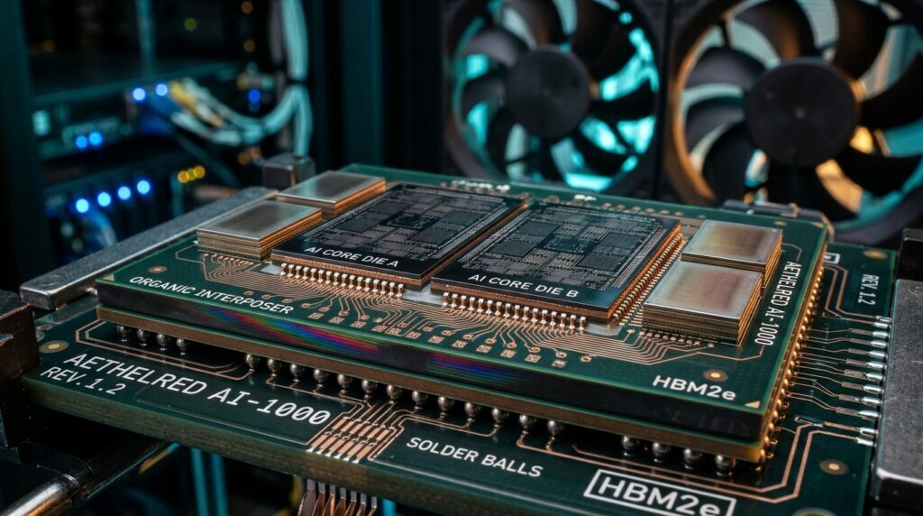
TSMC’s current flagship packaging for high-performance AI silicon is CoWoS-L (Chip-on-Wafer-on-Substrate with Local Silicon Interconnect). Unlike older CoWoS-S, which used a monolithic, brittle, and prohibitively expensive silicon interposer, CoWoS-L embeds tiny passive silicon bridges inside a flexible organic Redistribution Layer (RDL) interposer.
On paper, CoWoS-L was supposed to scale indefinitely. In reality, packaging a four-die substrate created an insurmountable physical failure mode: Coefficient of Thermal Expansion (CTE) mismatch.
The linear thermal expansion differential governing package stress is described by:
- Silicon Logic & Bridges (αsilicon): ≈ 2.6 × 10⁻⁶ / K
- Organic RDL Substrate (αsubstrate): ≈ 15.0 to 18.0 × 10⁻⁶ / K
- Expansion Delta (Δα): ≈ 12.4 to 15.4 ppm/K
When an assembled mega-package cools down from reflow temperatures (220°C) to ambient room temperature, the organic substrate contracts nearly six times faster than the rigid silicon chiplets bonded on top of it. Across a 3.3× reticle package like the dual-die Blackwell B200, this differential contraction causes manageable bowing that can be mitigated by underfill resin and stiffener rings.
Across a massive 12× to 14× reticle footprint, however, the mechanical moment of inertia breaks down. The substrate bows into a severe, non-linear “potato chip” curvature. During thermal cycling between idle states (40°C) and peak sustained compute (85°C–95°C), the lateral shearing stress exerted on the 25-micron copper pillar micro-bumps shears solder joints clean off their pads.
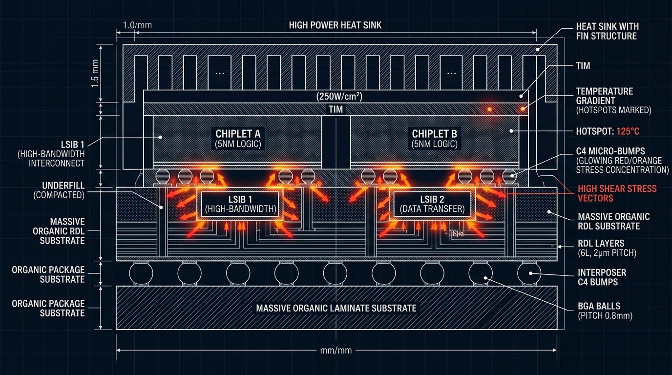
In finite-element simulations and early packaging trial runs, packaging yields for the four-die Rubin Ultra cratered to unviable single digits. Rather than risk catastrophic production delays similar to the early Blackwell mask respin, Nvidia’s engineering leadership made the pragmatic call: cancel the 4-die Rubin Ultra and freeze the architecture at a dual-die package.
The 17% Fan Tax: Inside the MGX GB200A NVL36 Air Rack
While packaging engineers battled thermal expansion at the micron scale, datacenter facility operators were revolting against fluid dynamics at the meter scale.
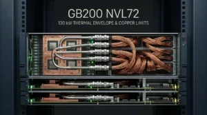
Nvidia originally architected the Blackwell generation around a single flagship topology: the GB200 NVL72, a monolithic 72-GPU rack drawing an astonishing 120kW to 132kW of electrical power. At that power density, air cooling is mathematically and thermodynamically impossible. Cooling 120kW with forced air would require hurricane-force airflow exceeding 95 decibels, creating acoustic shockwaves that damage mechanical hard drives and structural server chassis.
However, deploying liquid cooling at scale across brownfield enterprise datacenters proved to be a logistical and operational disaster. Field testbeds suffered from repeated plumbing failures:
- Quick-Disconnect (QD) Drip Rates: Blind-mate liquid quick-disconnect couplings connecting server trays to rear coolant manifolds exhibited unacceptably high micro-leak rates during hot-swap maintenance cycles.
- Manifold Alignment Shear: Rack-level thermal expansion caused 2U tray mounting rails to shift slightly relative to the vertical distribution manifold, placing bending moments on welded fluid joints.
- Cooling Distribution Unit (CDU) Lead Times: Severe shortages of enterprise-grade CDUs, secondary pumps, and treated water-glycol filtration loops left completed compute racks sitting unpowered on warehouse floors.
The Emergency Fallback: The 40kW MGX Air Compromise
Faced with customer pushback and delayed deployment schedules from cloud providers who lacked facility-wide liquid infrastructure, Nvidia had to engineer an emergency air-cooled alternative: the MGX GB200A NVL36.
To make air cooling remotely viable, Nvidia replaced the dual-die B200 with the B200A (B102)—a single monolithic die packaged on mature CoWoS-S, throttled to roughly 700W TDP and flanked by four HBM3E stacks. By halving the GPU density, Nvidia squeezed 36 B200A GPUs into an air-cooled 40kW rack envelope.
But the thermodynamic cost of brute-forcing 40kW of heat out of a standard server chassis using forced air is staggering:
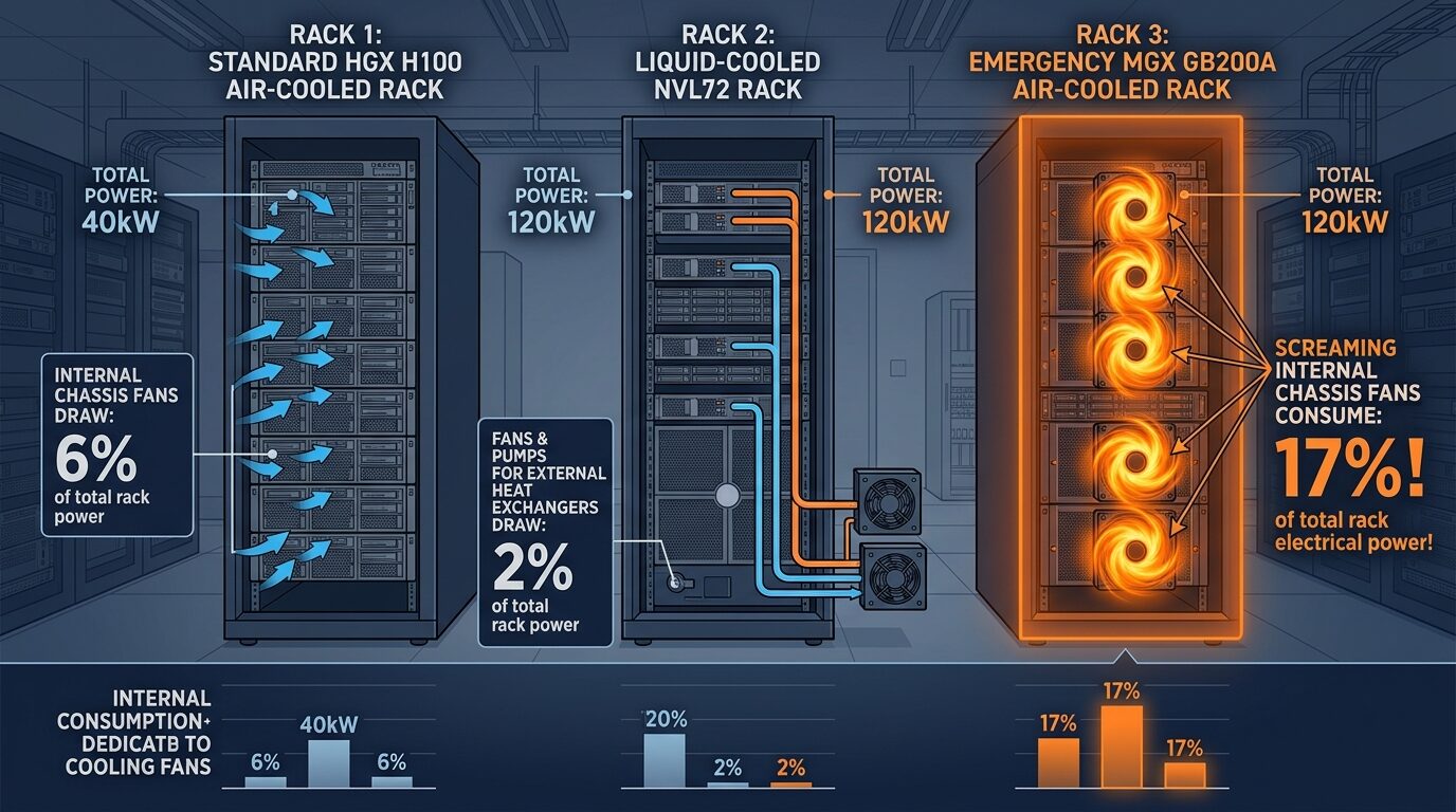
In a standard Hopper HGX H100 rack (drawing roughly 15kW to 20kW), internal chassis fans consume between 6% and 8% of the server’s electrical load. In the liquid-cooled NVL72, server-level fans draw almost zero power, with external heat exchanger blowers accounting for under 2% of total facility energy.
In the MGX GB200A NVL36, however, server engineers had to pack banks of dual-rotor, counter-rotating 60mm and 80mm delta fans spinning at 24,000 to 26,000 RPM directly in front of and behind custom 3D vapor chambers. Under sustained training loads, these screaming fan walls consume 6.2 kW to 6.8 kW per rack.
| ARCHITECTURE & TOPOLOGY | TOTAL RACK POWER | COOLING MECHANISM | FAN POWER DRAW | THE “FAN TAX” RATIO |
|---|---|---|---|---|
| HGX H100 (8x SXM5) | 15 kW – 20 kW | Conventional Air | 0.9 kW – 1.4 kW | 6.0% – 7.5% |
| GB200 NVL72 (72x B200) | 120 kW – 132 kW | Direct-to-Chip Liquid | 1.8 kW – 2.4 kW (Facility) | 1.5% – 2.0% |
| MGX GB200A NVL36 (36x B200A) | ~40 kW | High-Pressure Air Forced | 6.2 kW – 6.8 kW | 15.5% – 17.0% |
This is the 17% Fan Tax: customers buying the air-cooled GB200A rack to avoid the headaches of liquid plumbing are sacrificing nearly a fifth of their power bill just to produce noise and blow warm air across heatsinks. In hyperscale clusters where power substations are capped at 50MW or 100MW, paying a 17% energy penalty on fans directly reduces the number of compute nodes that can be deployed within that power envelope.
The Autopsy of the Scrapped NVL64
Before settling on the 40kW NVL36, Nvidia spent months attempting to make an intermediate 64-GPU air-cooled rack viable: the NVL64. That design called for drawing 65kW to 70kW out of a single air rack. It was ultimately scrapped for two fatal mechanical reasons.
First, the interconnect wiring created an aerodynamic blockade. In order to interconnect 64 GPUs with full all-to-all NVLink bandwidth, the chassis required thousands of Ultrapass copper twinax flyover cables connecting the GPU baseboards to the central NVLink switch trays. When routed through the backplane of the rack, these thick cable bundles formed a literal physical wall, choking the exhaust airflow and creating massive static pressure drops that no fan could overcome.
Second was the single point of failure dilemma. In an unpartitioned 64-GPU NVLink domain, if a single GPU throttles thermally or fails due to fan failure, the entire 64-node collective communication mesh stalls. Without the ability to hot-swap a compute tray without powering down the entire air-pressurized chassis, the operational SLA of NVL64 collapsed.
The HBM4 “NVHBM” Coup: Nvidia’s Base Die Margin Grab
While packaging and thermal engineers wrestle with physical hardware limits, Nvidia’s silicon architects are executing an unprecedented structural capture of the semiconductor value chain: NVHBM.
In High Bandwidth Memory generations through HBM3E, the memory cube consisted of vertical stacks of DRAM dies sitting atop a proprietary base (buffer) die fabricated directly by the memory vendor (SK Hynix, Samsung, or Micron) on a trailing DRAM process. The GPU communicated with the HBM stack over a standardized 1024-bit JEDEC bus.
With HBM4, the industry is transitioning to a massive 2048-bit interface, doubling the pin count to over 5,000 micro-bumps per stack. Because legacy DRAM processes cannot route that density or support advanced power management, the HBM base die must now be fabricated on high-performance CMOS logic foundry nodes (TSMC 4nm/3nm).
By partnering directly with TSMC to fabricate custom HBM4 base dies, Nvidia is moving the memory controller and physical layer (PHY) directly into the HBM base die itself:
- Captured by Nvidia & TSMC: Proprietary NVLink-HBM protocols, memory controller IP, PHY serialization, and high-margin silicon value.
- Pushed to Memory Vendors (SK Hynix, Micron): Multi-billion dollar DRAM wafer CapEx, complex 16-high microbump stacking, TSV (Through-Silicon Via) bonding defect risks, and thermal dissipation yield losses.
This shift cements Nvidia’s ecosystem lock-in. By deploying proprietary NVHBM signaling instead of standard JEDEC protocols, Nvidia gains up to 30% higher effective memory bandwidth and 15% lower memory interface power. But it simultaneously converts memory manufacturers from independent subsystem suppliers into contracted wafer stackers who must absorb the brutal yield losses of 16-high bonding.
The Glass Core Horizon: Why CoWoS Is Living on Borrowed Time
The cancellation of the 4-die Rubin Ultra and the 17% fan tax compromise prove one undeniable thesis: organic resin packaging has reached its physical limits.
If the AI industry is to scale processors beyond 4 reticles toward 10× and 14× reticle wafer-scale systems, the organic interposer must be completely abandoned. That is why TSMC, Intel, and advanced substrate leaders are racing toward Glass Core Substrates (GCS).
Glass delivers fundamental material properties that organic resins simply cannot match:
- Tunable Thermal Expansion: The CTE of specialized borosilicate and aluminosilicate glass can be engineered between 3.0 and 8.0 ppm/K, closely matching the 2.6 ppm/K of silicon and eliminating package warpage during reflow.
- Extreme Planarity & Stiffness: Glass provides over 4× higher flexural modulus than organic laminates, remaining atomically flat across massive 515mm × 510mm rectangular panel formats.
- Through-Glass Vias (TGV): Laser-drilled TGVs achieve sub-100nm sidewall roughness, enabling 112G and 224G high-speed interconnects with near-zero dielectric loss.
TSMC is already constructing its pilot CoPoS (Chip-on-Panel-on-Substrate) lines in collaboration with Japan’s Ibiden and display giant Innolux. But commercial high-volume glass panel packaging will not reach production readiness until late 2027 or 2028. Until then, the semiconductor industry must grind through a messy, multi-year transition era bounded by organic warpage, conservative chiplet die counts, and deafening datacenter fan walls.
The Systems Reality: What Builders and Buyers Need to Know
For engineering leaders, infrastructure buyers, and datacenter architects, this hardware inflection delivers three immutable operational takeaways:
- Beware the “Air-Cooled Compromise”: If your enterprise facility lacks direct-to-chip liquid cooling and you are considering 40kW air-cooled racks like the MGX GB200A NVL36, account for the 17% fan power penalty in your TCO models. You are paying tier-1 electrical rates to spin fans, not generate tokens. Model your actual workload economics using our AI Coding Cost Calculator.
- Liquid Cooling Is No Longer Optional Above 40kW: Despite the early headaches with quick-disconnect fittings and CDU supply chains, liquid cooling is the only thermodynamically viable path for frontier density. Facilities that delay retrofitting liquid manifolds will find themselves completely shut out of 2026/2027 compute allocations.
- The Die-Count Stagnation Window: With Rubin Ultra constrained to two compute dies, raw per-socket monolithic compute scaling has plateaued until glass substrates arrive. Near-term performance gains will come from architectural efficiency, compiler optimizations, and test-time search loops rather than brute-force package expansion.
References & Technical Source Verification
This investigation was compiled using primary foundry documentation, published packaging patents, and independent semiconductor telemetry:
- TSMC CoWoS-L Technical Architecture: TSMC Advanced Packaging Technology Symposium (Micro-bump pitch, RDL layer limits, and LSI bridge specifications).
- SemiAnalysis Hardware Rework Telemetry: Dylan Patel, “Nvidia’s Blackwell Reworked: CoWoS-L, Liquid Cooling vs. Air Cooling, and the GB200A Compromise” (August 2024 – September 2026).
- Thermal Expansion Material Constants: IEEE Transactions on Components, Packaging and Manufacturing Technology (Silicon CTE 2.6 ppm/K vs ABF Organic Buildup Substrates 15–18 ppm/K).
- Datacenter Fan Power Telemetry: ASHRAE Technical Committee 9.9 Data Center Power Trends & Fan Affinity Laws for high-density 40kW air-cooled compute chassis.
- Related Eyestech Research: Jaxson Reed’s M4 Pro Mac Mini Bare-Metal Teardown and Elena Rostova’s Astra Latency Trap Architecture Audit.