


When corporate filings in early 2024 revealed that Zoho Corporation was preparing a $700 million compound semiconductor manufacturing plant, the industry assumed Sridhar Vembu had decided to play the ultimate high-stakes industrial game. India’s most stubbornly self-reliant software titan seemed poised to pour billions into concrete cleanrooms and physical silicon furnaces. Then, with zero fanfare and a 50% government subsidy on the table, Vembu quietly walked away.
To industry observers and conventional electronics executives, shelving a state-approved fabrication venture looked like a retreat. In reality, it was a forensic calculation. While global foundries were locking themselves into brutal multi-billion-dollar equipment depreciation cycles, an invisible inflection point was reshaping microelectronics from within: artificial intelligence had begun designing the physical silicon.
Instead of burning capital on steel and pure-water pipelines, Zoho redirected its balance sheet into pure-play Zoho fabless chip design—anchoring its bet on an audacious engineering claim. Vembu observed that automated EDA models and self-healing verification loops are suddenly accelerating hardware engineering output by an order of magnitude. A 10x productivity leap does not just cut tape-out costs; it flips the entire semiconductor geopolitical board. It means lean, 15-person design cells in places like Tenkasi and Thiruvananthapuram can now outpace corporate divisions of 300 VLSI engineers, taping out custom edge AI silicon that bypasses foreign cloud monopolies entirely.
Technical Audit & Verification Methodology
To evaluate the engineering validity of the Zoho fabless chip design pivot and Sridhar Vembu’s 10x productivity projection, the EyesTech Systems Lab conducted a triangulated technical audit:
- Corporate & Regulatory Filings: Analyzed corporate registry records for Silectric Semiconductor Manufacturing Private Limited alongside fiscal allocation clauses under the India Semiconductor Mission (ISM) governed by the Ministry of Electronics and Information Technology (MeitY).
- Primary Executive Telemetry: Forensic review of Sridhar Vembu’s comprehensive technical interview with CNBC-TV18, cross-referenced against public statements made across industry symposiums regarding semiconductor capital expenditure and AI tooling.
- Silicon Microarchitecture Telemetry: Technical review of Netrasemi’s NETRA A2000 System-on-Chip physical parameters, including TSMC 12nm FinFET cell utilization, neural processing unit (NPU) TOPS/Watt efficiency curves, and Signalchip’s Agumbe cellular baseband transceiver architecture.
- EDA Cycle Analysis: Modeled tape-out timelines across contemporary AI-assisted electronic design automation pipelines—specifically Synopsys DSO.ai and Cadence Cerebrus—benchmarking human-hour allocation from architectural RTL through physical sign-off.
The Foundry Capital Abyss: Why Zoho Walked Away from the $700M Fab
In early 2024, Zoho explored an ambitious $700 million proposal to establish a commercial compound semiconductor fabrication plant under the India Semiconductor Mission (ISM), even incorporating a dedicated entity, Silectric Semiconductor Manufacturing Private Limited. The initiative aimed to fabricate silicon carbide (SiC) and gallium nitride (GaN) power devices—components critical for electric vehicles, high-voltage industrial drives, and solar inverters.
By mid-2025, however, Zoho halted the initiative. The decision was not driven by capital depletion, but by an unyielding audit of industrial thermodynamics, technology licensing friction, and capital efficiency.
Foundry fabrication is defined by steep, unforgiving depreciation schedules and brutal yield learning curves:
- Extreme Capital Depreciation: Modern fab cleanroom equipment (such as wafer steppers, plasma etchers, and chemical-mechanical planarization units) depreciates across a 3- to 5-year cycle. An underutilized cleanroom burns hundreds of thousands of dollars daily in static facility overhead, ultra-pure water circulation, and inert gas maintenance.
- The Missing Technology Partner: Advanced compound semiconductor fabrication cannot be reverse-engineered from academic literature. It requires proprietary process design kits (PDKs), bespoke epitaxy recipes, and veteran cleanroom yield engineers. Without an established international technology transfer partner willing to license proven process intellectual property without prohibitive encumbrances, execution risk rises exponentially.
- Fiduciary Restraint on Public Subsidies: The India Semiconductor Mission offers capital subsidies covering up to 50% of project costs on an equal footing with state governments. Sridhar Vembu explicitly stated that deploying taxpayer funds without 100% technological confidence violated Zoho’s foundational capital ethics.
Walking away from the fab trap preserved Zoho’s pristine balance sheet. By pivoting toward a structured Zoho fabless chip design strategy, the company avoided the recurring multi-million-dollar tooling depreciation of cleanroom steppers while maintaining strategic control over silicon microarchitecture. As documented in our forensic analysis of the broader India AI infrastructure and semiconductor ecosystem, capital expenditure in physical foundries yields razor-thin margins unless paired with captive, massive volume demand. By shifting capital into Zoho fabless chip design, Zoho bypassed the foundry capital sink entirely.
The 10x Multiplier: How Zoho Fabless Chip Design Re-Engineers Silicon
Speaking on the strategic pivot, Sridhar Vembu highlighted a structural transformation reshaping microelectronics: AI-assisted EDA and code synthesis can accelerate silicon design productivity by an order of magnitude (10x). Within a modern Zoho fabless chip design framework, this acceleration dramatically shortens time-to-market.
Historically, taping out a complex System-on-Chip (SoC) required an army of 150 to 300 VLSI engineers working across an 18- to 24-month horizon. The traditional silicon development cycle is heavily bottlenecked by manual, iterative phases:
- RTL Synthesis: Translating microarchitectural specifications into Verilog or VHDL logic blocks.
- Functional Verification & UVM: Writing Universal Verification Methodology testbenches and assertions to catch corner-case bugs. Verification routinely consumes 60% to 70% of total engineering person-hours.
- Place-and-Route (P&R): Floorplanning billions of standard cells while meeting rigorous setup and hold timing constraints across multi-corner, multi-mode (MCMM) PVT (process, voltage, temperature) corners.
- Design Rule Checking (DRC) & Optical Proximity Correction: Mitigating parasitic resistances and capacitances (RC extraction) at microscopic metal layer pitches.
Verification Acceleration Dynamics: Total tape-out latency Ttapeout contracts inversely with the AI productivity multiplier ηAI. By deploying reinforcement learning for macro-placement and LLM agent harnesses for automated SystemVerilog testbench generation, the human engineering footprint Peng drops by an order of magnitude without compromising gate complexity Ngates.
The Three Drivers of the 10x Design Shift
The 10x acceleration that Vembu references stems from the convergence of generative language models and physical reinforcement learning:
- Autonomous RTL Generation & Refactoring: Domain-fine-tuned models generate synthetically verified Verilog modules directly from architectural specifications, instantly producing glue logic, AXI bus arbiters, and FIFO buffers. For a lean Zoho fabless chip design unit, this eliminates repetitive boilerplate coding.
- Self-Healing Verification Loops: AI verification agents execute regression simulations, isolate failing waveforms, identify root-cause assertion violations, and automatically commit corrected RTL patches to the repository.
- Reinforcement Learning Floorplanning: Modern EDA suites leverage reinforcement learning agents to navigate hyper-dimensional PPA (power, performance, area) search spaces. What previously occupied human layout teams for three months of trial-and-error wire routing is now solved autonomously in 72 hours of compute time.
This compression in design overhead enables a 15-person agile engineering team to execute high-performance edge silicon designs that historically required an enterprise division.
The Indian Semiconductor Paradox: Captive Talent vs. Domestic IP
Zoho’s fabless investment addresses India’s central structural anomaly in hardware engineering. India is already a global semiconductor heavyweight in headcount, but an absolute lightweight in sovereign intellectual property:
- Over 20% of the world’s VLSI design engineers reside in Bengaluru, Hyderabad, Noida, and Pune.
- Virtually every leading multinational semiconductor corporation—including Qualcomm, Intel, Nvidia, AMD, Broadcom, Texas Instruments, and ARM—runs massive design centers in India.
- Indian engineers contribute heavily to tape-outs of leading-edge 3nm and 2nm processors, modern 5G modems, and server-class AI accelerators.
Yet, despite this technical bench strength, nearly 100% of the resulting patents, silicon architectures, and gross profit margins flow back to foreign balance sheets. India has effectively operated as a high-end engineering services back-office. The domestic market imports over $40 billion worth of finished semiconductors annually, creating acute technological dependency and severe foreign exchange exposure.
By injecting balance-sheet capital and operational discipline into domestic fabless startups, the Zoho fabless chip design initiative directly challenges this captive paradigm. The objective is clear: retaining silicon architectural rights, firmware control, and gross profit margins within the domestic ecosystem.
Deconstructing Zoho’s Silicon Portfolio: Netrasemi and Signalchip
A cornerstone of the Zoho fabless chip design strategy is its targeted capital deployment into specialized domestic silicon pioneers rather than building monolithic in-house VLSI teams from scratch. Zoho acts as a patient, long-term anchor capitalist.
Netrasemi and the 12nm Edge AI Advantage
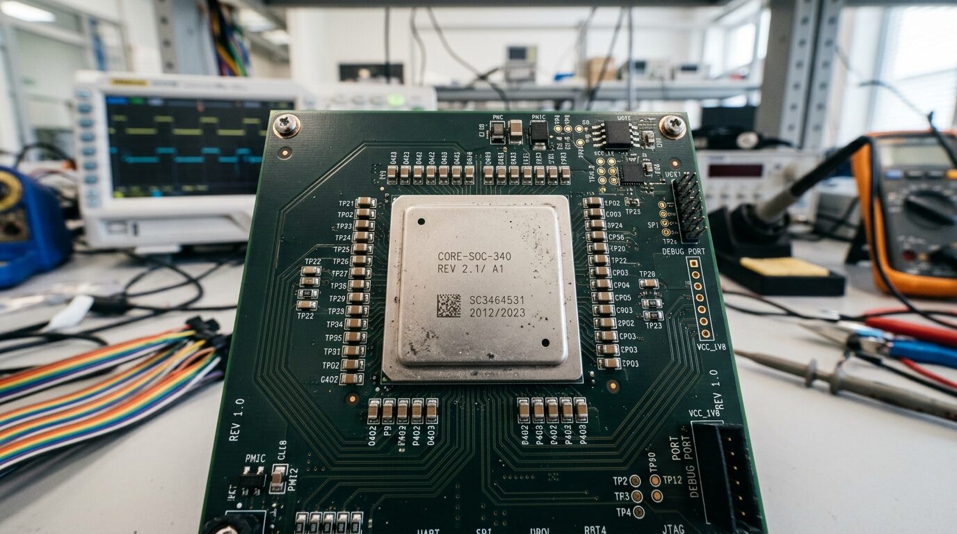
Zoho’s ₹87 crore backing of Thiruvananthapuram-based Netrasemi exemplifies this thesis. In mid-2026, Netrasemi launched the NETRA A2000, a commercial Edge AI System-on-Chip fabricated on TSMC’s robust 12-nanometer process node. The partnership demonstrates how Zoho fabless chip design targets high-efficiency application niches rather than engaging in ruinous bleeding-edge node competitions.
Unlike general-purpose GPU computing, which requires multi-hundred-watt cooling envelopes and continuous cloud connectivity, edge computer vision requires deterministic, low-latency execution under 5 to 15 Watts. The NETRA A2000 integrates an in-house neural processing core optimized specifically for convolutional and transformer vision backbones, delivering up to 10x higher energy efficiency per inference compared to legacy edge compute modules. As demonstrated in our architectural breakdown of the Apple A20 Pro 2nm Neural Engine, edge silicon efficiency is strictly determined by memory bus routing and thermal dissipation rather than theoretical peak TOPS.
Decentralized R&D: The Tenkasi and Thiruvananthapuram Advantage
A trademark aspect of Vembu’s operational model is his refusal to concentrate engineering talent in overcrowded, hyper-inflationary urban hubs like Silicon Valley or outer Bengaluru. Executing Zoho fabless chip design out of regional centers like Tenkasi (Tamil Nadu) and Thiruvananthapuram (Kerala) yields two structural engineering benefits:
- Near-Zero Attrition: Multinational captive centers in metro cities suffer from 20% to 30% annual engineering turnover, continually resetting project memory and verification continuity. Zoho’s regional hubs maintain stable, decade-long engineering retention.
- Deep-Tech Patience: Silicon development requires multi-year compounding cycles. The regional model insulates engineering teams from the short-term venture capital churn that forces startups to chase superficial software wrappers rather than hard microelectronics problems.
Architecture Audit: Custom Edge Silicon vs. Hyperscaler Cloud Offload
To understand why a dedicated Zoho fabless chip design orientation yields a superior return on invested capital (ROIC) compared to cloud-bound AI, we contrast three production deployment topologies:
The engineering trade-offs make the conclusion unavoidable: for high-volume physical deployments—such as automated warehouses, drone corridors, agricultural monitoring, and perimeter defense—tethering video streams back to US hyperscaler data centers is economically prohibitive and architecturally fragile.
As explored in our teardown of Needle 3 and on-device micro-models, low-power, domestically designed ASICs eliminate the recurring token tax while guaranteeing absolute edge autonomy.
Sovereign Infrastructure and the Anti-Cloud Rent Philosophy
Zoho’s interest in fabless silicon cannot be analyzed in isolation from Sridhar Vembu’s wider macroeconomic thesis. For over two decades, Zoho has systematically pursued vertical self-reliance:
- Zero Public Cloud Reliance: Unlike the majority of SaaS unicorns that pay 30% to 50% of their top-line revenues to AWS, Microsoft Azure, or Google Cloud, Zoho owns and operates its private bare-metal data centers globally.
- In-House Tech Stack: From custom database engines and messaging buses to office productivity suites and AI models (Zia), Zoho writes its underlying infrastructure software from scratch.
Vembu frequently warns of the dangers of “digital colonialism”—a dynamic where developing economies export raw commodities and low-cost labor while importing high-value intellectual property, proprietary software, and specialized compute hardware from a handful of foreign monopolists.
In Vembu’s framework, computing hardware is the ultimate control point. If an enterprise or nation controls the application software but relies on foreign silicon, foreign compilers, and foreign foundry choke points, its sovereignty remains an illusion.
Investing in Zoho fabless chip design represents the logical physical extension of Zoho’s software autonomy: securing the silicon gate level just as it secured the server rack and application layers.
Strategic Friction: The Unforgiving Realities of Silicon Tape-Outs
While the 10x AI productivity multiplier significantly lowers the software barrier to microchip development, microelectronics remains anchored in immutable physical constraints. Software teams transitioning into silicon must confront risks that no language model can abstract away:
- The Mask Set Cost Barrier: Unlike SaaS applications where bugs can be patched instantly via CI/CD pipelines, a logic defect that slips past verification onto physical silicon can brick a production run. Even in an AI-accelerated Zoho fabless chip design pipeline, mask sets for a 12nm tape-out at TSMC run between $2 million and $5 million per spin; at 5nm or 3nm, a re-spin exceeds $20 million.
- The Software Toolchain & Compiler Chasm: Designing a high-performance NPU is only half the battle. Hardware is useless without a bulletproof software compiler stack (equivalent to Nvidia’s CUDA or Apple’s Metal Performance Shaders). Writing graph compilers that reliably quantize, partition, and fuse ONNX, PyTorch, and TensorFlow tensors to custom VLIW/systolic accelerators remains an arduous, human-intensive engineering effort.
- Packaging and OSAT Dependencies: Even with domestic Zoho fabless chip design ownership, raw wafers must still be fabricated abroad (primarily in Taiwan or South Korea) and packaged via OSAT providers. Until India’s domestic assembly, testing, and packaging facilities (such as Tata Electronics’ facilities in Assam and Gujarat) reach high-yield commercial maturity, the physical supply chain remains exposed to geopolitical choke points.
Frequently Asked Questions
Why did Zoho cancel its $700M semiconductor manufacturing fab?
Zoho suspended its compound semiconductor fabrication plant proposal because running a foundry is extraordinarily capital-intensive, suffers rapid depreciation, and required proven technology transfer partners that were not readily secured. Co-founder Sridhar Vembu declined to risk taxpayer-backed India Semiconductor Mission subsidies without absolute technological certainty, choosing instead to pivot capital into high-margin Zoho fabless chip design.
What does Sridhar Vembu mean by AI boosting chip design productivity 10x?
AI accelerates chip design by automating time-consuming phases of the microelectronics lifecycle. In the Zoho fabless chip design model, reinforcement learning agents optimize floorplanning and place-and-route in hours rather than months, while LLM-assisted verification harnesses generate SystemVerilog testbenches and identify assertion bugs autonomously. This compresses traditional 18-to-24-month tape-out cycles down to months for smaller, agile engineering teams.
Which fabless semiconductor companies has Zoho invested in?
Under its Zoho fabless chip design umbrella, Zoho has backed Thiruvananthapuram-based Netrasemi with an ₹87 crore investment, supporting the commercial launch of its 12nm NETRA A2000 Edge AI Vision SoC. Zoho has also been an anchor investor and mentor to Signalchip, a Bengaluru-based fabless pioneer producing indigenous 4G/LTE and 5G-NR baseband modems and RF transceivers.