

On September 8, 2026, Qualcomm Technologies and Amazon Web Services formalized a multi-generational silicon pact carrying a potential procurement ceiling of $60 billion over ten years, anchored by Qualcomm’s AI200 and AI250 accelerators (the “Dragonfly” portfolio), co-developed optical interconnects reaching 1.6 Tbps, and an equity warrant granting Amazon the right to acquire up to 25 million Qualcomm shares. This is a vertically integrated hardware thesis: Qualcomm bringing its Hexagon NPU lineage, its 2025 Alphawave Semi acquisition (SerDes + optical DSP), and its newly acquired Modular/MAX inference engine to bear directly on AWS’s hyperscale inference bottleneck — while Amazon weaponizes its Bedrock EDA tools to compress Qualcomm’s chip design cycles.
1. Why AWS Needed a Third Pillar
AWS already operates two custom silicon lineages: Trainium (training/high-performance inference, now Trn2) and Inferentia (inference ASIC, now Inf2, with documented 25–40% lower cost-per-token vs NVIDIA G5 instances). Both are internally designed. They carry two structural vulnerabilities that the Qualcomm pact is engineered to resolve.
Single silicon supply chain entirely dependent on AWS internal tape-outs at TSMC. A single fab disruption — earthquake, geopolitical embargo, yield collapse — creates a direct hyperscaler SLA breach.
Nitro/EFA fabrics cap before the physical limits of photonic solutions at frontier-model scale. As context windows stretch beyond 512K tokens, KV-cache eviction becomes the primary inference cost driver.
Qualcomm’s Alphawave Semi acquisition (Q1 2025, ~$5.8B) provides exactly what AWS lacks: production-grade SerDes IP, coherent optical DSP silicon, and a roadmap to 1.6 Tbps lane-level optical connectivity. The resulting three-pillar portfolio:
2. Dragonfly Portfolio Architecture
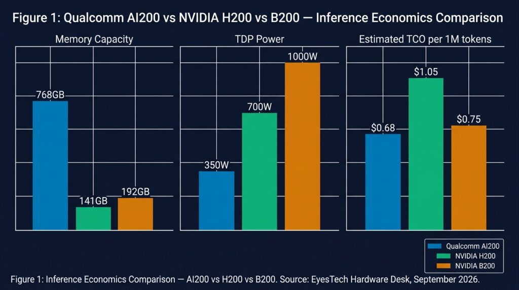
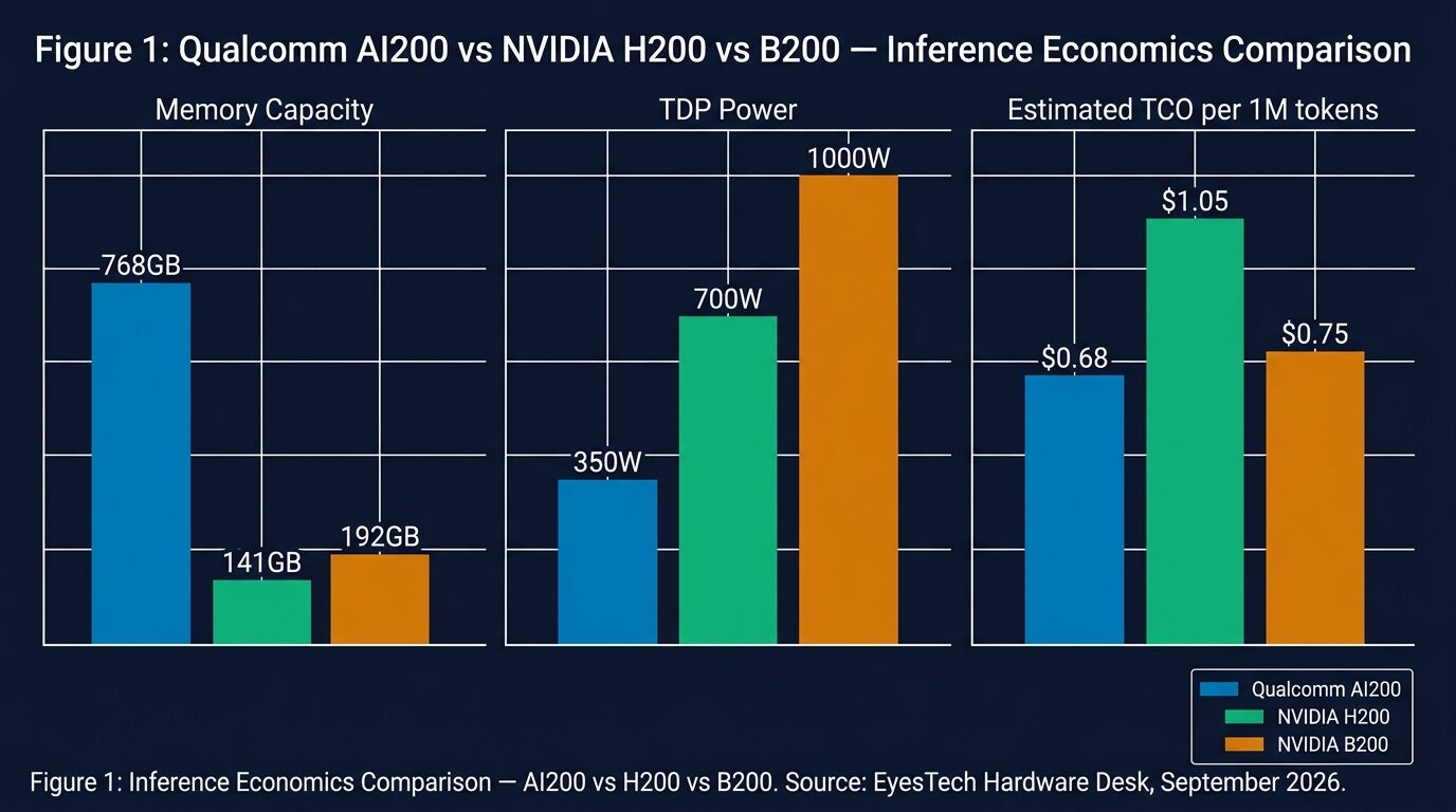
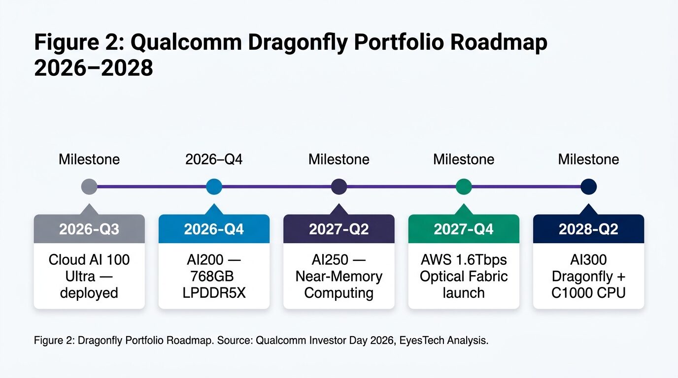
The Dragonfly roadmap spans five chip generations across six years, each stage advancing on a different axis of inference limitation — from raw memory capacity to photonic coherence at rack scale. The AI200 carries 768 GB LPDDR5X vs H200’s 141 GB HBM3e and B200’s 192 GB HBM3e — a 4–5× capacity advantage enabling unsharded 70B model inference on a single card.
| Chip Generation | Availability | Memory Configuration | Architectural Innovation | Strategic Role |
|---|---|---|---|---|
| Cloud AI 100 Ultra | Deployed | HBM2E / LPDDR5 | Established Hexagon NPU inference; proven at hyperscale via cloud CSP deployments | AWS migration baseline; existing fleet anchor |
| Qualcomm AI200 | 2026 | 768 GB LPDDR5X | On-card model residency — full 70B parameter set fits without tensor parallelism across cards | Primary AWS Bedrock inference instance; HUMAIN anchor |
| Qualcomm AI250 | 2027 | Near-Memory Computing | Bandwidth wall breaker — compute logic embedded adjacent to DRAM arrays, eliminating data movement bottleneck | Frontier-model context scaling; 405B+ unsharded target |
| Qualcomm AI300 | 2028 | HBC (Hybrid Bandwidth Chip) | Photonic coherence — full 1.6 Tbps optical fabric natively integrated; rack-scale inference mesh | AWS optical inference fabric anchor; sovereign AI deployments |
| Dragonfly C1000 CPU | 2028 | N/A (CPU) | 250-core Oryon server CPU — ARM-native data center compute displacing Graviton in AI-adjacent workloads | Orchestration layer; Graviton competitive displacement |
3. The AI200 Memory Bet
The defining architectural gamble of the Dragonfly portfolio is its memory subsystem philosophy: Qualcomm bets on capacity (768 GB LPDDR5X) over bandwidth density (HBM3e). This is a deliberate inference-economics thesis — at serving time for 70B models, the binding constraint is model weight residency, not peak bandwidth. The three-way comparison:
4. The 1.6 Tbps Optical Interconnect
Alphawave’s zMorph PHY (sub-7nm, 224G PAM4) enables coherent optical interconnects targeting 1.6 Tbps per lane aggregate — 2–4× beyond today’s deployed EFA generations — keeping large KV caches on-rack without cross-cluster eviction. This is a three-layer silicon stack:
Serializer/Deserializer blocks operating at 224G PAM4 symbol rates. Production-grade IP from the Alphawave portfolio (sub-7nm process). Provides the electrical signaling foundation before electro-optical conversion.
Digital Signal Processor for coherent optical modulation — converts electrical PAM4 signals to DP-16QAM optical format. Enables multi-km reach at rack-scale without signal degradation. The Alphawave acquisition unlocks this layer for Qualcomm.
Full-stack PHY integrating SerDes, clock-data recovery, forward error correction, and optical DSP into a single monolithic silicon block. Enables plug-and-play 1.6 Tbps connectivity without discrete optical module assembly.
The 1.6 Tbps optical fabric is a 2027–2028 capability tied to AI300 general availability. Current Qualcomm AI200 deployments (2026) remain on 400G EFA/InfiniBand for inter-card traffic. Engineers evaluating AI200 instances on AWS Bedrock should not expect optical-native interconnects until the AI300 generation.
5. Inference Cost Economics
The economic thesis is clear: AI200’s lower TDP yields $8.75M–$17.5M annual electricity savings at 1,000-card deployments vs H200 at standard colocation rates ($0.08–0.12/kWh). The complete seven-metric comparison:
| Metric | Qualcomm AI200 | NVIDIA H200 | NVIDIA B200 |
|---|---|---|---|
| Total Memory | 768 GB LPDDR5X ✓ | 141 GB HBM3e | 192 GB HBM3e |
| Memory Bandwidth | ~1.4 TB/s | 4.8 TB/s ✓ | 8.0 TB/s ✓✓ |
| Thermal Design Power | ~300–400W ✓ | 700W | 1,000W ⚠ |
| Est. TCO / 1M tokens (70B model) | $0.55–$0.80 ✓ | $0.90–$1.20 | $0.65–$0.85 |
| 70B Unsharded (Single Card) | Yes ✓ | No — 2+ cards required | No — 2 cards required |
| Annual Electricity Cost (1,000 cards @ $0.10/kWh) | ~$3.1M–$3.5M ✓ | ~$6.1M | ~$8.8M ⚠ |
| Interconnect Fabric | 400G EFA (2026) → 1.6 Tbps optical (2028) | NVLink 4 / InfiniBand NDR | NVLink 5 / InfiniBand HDR |
6. Modular/MAX Engine: The CUDA Moat Answer
MAX (Mojo-based, from the Modular acquisition) compiles silicon-agnostic inference kernels across CUDA, Hexagon NPU, ARM, and ROCm backends. The practical engineer story: a single Python/Mojo inference pipeline generates optimized AI200 kernels without a CUDA rewrite. This is the first credible answer to NVIDIA’s decade-long CUDA ecosystem moat for teams running 70B+ parameter models.
The compiler stack generates optimized kernels via a unified IR (intermediate representation) that targets each backend’s native instruction set — Hexagon VLIW for AI200, PTX for CUDA GPUs, and ARM SVE for server CPUs — enabling performance portability without per-hardware kernel engineering.
The Modular/MAX package registry introduces a new supply chain attack surface that security teams must audit before any production rollout.
Treat MAX kernel compilation provenance with the same scrutiny applied to npm’s documented gap in the DeepSeek CVE-2026-82533 patch deployment. Specifically: (1) pin MAX package versions and verify SHA-256 digests against Modular’s published registry; (2) run kernel compilation in isolated Firecracker microVM sandboxes before fleet-wide deployment; (3) implement out-of-band cryptographic attestation for compiled kernel artifacts before loading onto AI200 cards in production. The CUDA ecosystem has 15 years of supply chain hardening. The MAX ecosystem does not.
7. HUMAIN: The 200MW Sovereign AI Deployment
8. The $15B Revenue Target: A Reality Check
Qualcomm’s FY2029 data center revenue target of $15B requires approximately 19× growth in three years from a ~$800M 2025 baseline. The path is credible on paper — but carries a single fatal dependency: hyperscaler-grade uptime SLAs and 24/7 enterprise support cadence that Qualcomm has never operated at this scale.
The AWS deal requires Qualcomm to deliver hyperscaler-grade 99.99% uptime SLAs, multi-region support coverage, and enterprise incident response at a scale Qualcomm has never operated. The technology is credible; the operational execution is the binding constraint.
9. Implications for Engineers
Three distinct engineering audiences face materially different decisions in light of the Qualcomm × AWS pact. Here is the forensic breakdown for each:
By EyesTech Systems Architecture & Hardware Desk — Published September 10, 2026. Entity scope: Qualcomm Technologies Inc. / Amazon Web Services / Qualcomm AI200 / Dragonfly Portfolio / Alphawave Semi. This analysis draws on publicly disclosed deal terms, Qualcomm investor materials, AWS silicon roadmap presentations, and Alphawave technical specifications current as of filing date.