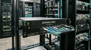


DeepSeek is deploying 160,000 Huawei Ascend 950DT AI accelerators across a gigawatt-scale computing campus in Ulanqab, Inner Mongolia to pre-train a planned 8-trillion-parameter sparse Mixture-of-Experts model. During closed-door Series B briefings on September 21, 2026, CEO Liang Wenfeng told investors that transitioning pre-training to domestic silicon “has to work.” This marks the first attempt in AI history to train a multi-trillion-parameter frontier model entirely outside the Western semiconductor supply chain.
| Cluster Metric | Forensic Value | Engineering Source & Architecture Notes |
|---|---|---|
| Accelerator Allocation | 160,000 NPU Units | Huawei Ascend 950DT series deployed in Ulanqab, Inner Mongolia |
| Frontier Model Target | 8 Trillion Parameters | Ultra-sparse MoE (~80B–140B active parameters per forward pass) |
| Current Pre-Training Run | 2 Trillion Parameters | Active run; serving as algorithmic baseline for 8T cluster scaling |
| Per-Chip FP8 Throughput | ~1.0 PFLOP (FP8) | Dual-chiplet compute complex; ~2.0 PFLOPS under native MXFP4 |
| Memory Architecture | 144 GB HiZQ 2.0 HBM | ~4.0 TB/s bandwidth; proprietary domestic stacked DRAM on 2.5D interposer |
| Process Lithography | SMIC N+2 / N+3 (7nm DUV) | Self-Aligned Quadruple Patterning (SAQP); zero EUV dependency |
| Delivery Window | Q4 2026 – Q1 2027 | Committed delivery; Ascend 960DT rejected due to late-2027 schedule |
| Cluster Topology | ~20× Atlas 950 SuperPoDs | 8,192 NPUs per SuperPoD; UnifiedBus intra-pod, RoCEv2 optical inter-pod |
| Continuous Power Budget | >100 MW – 120 MW | ~600W–750W TDP per chip; 100% direct-to-chip liquid cooling |
| Series B Capital Raise | 50B Yuan (~$7.5B USD) | Post-money valuation of 500B Yuan (~$75B USD); earmarked for silicon procurement |
| Huawei Foundry Allocation | ~66% Combined Share | DeepSeek and ByteDance absorb two-thirds of Huawei’s total 2026 AI silicon capacity |
| Unit Hardware Pricing | >250,000 Yuan / Unit | Domestic demand squeeze; total silicon order value exceeds 40B Yuan ($5.7B) |
Liang Wenfeng’s Closed-Door Admission Changed Everything
On September 21, 2026, The Information broke the story that altered the strategic calculus of the global AI chip war: DeepSeek CEO Liang Wenfeng—speaking during closed-door briefings for the firm’s Series B capital raise—told key institutional investors that transitioning model pre-training from Nvidia hardware to domestic Chinese silicon was no longer a research hedge. It has become the company’s existential priority. According to attendees, Liang’s exact words were unequivocal: the pivot to domestic hardware “has to work.”
Those three words carry immense weight. Earlier this month, our forensic teardown of DeepSeek’s enterprise trajectory (The $75 Billion Breakout: Inside DeepSeek’s Critical CVE-2026-82533 Sandbox Escape and STAR Market IPO Rush) traced how Liang’s quantitative trading background at High-Flyer Capital shaped an organization uniquely obsessed with unit economics and architectural efficiency. But capital alone cannot bypass physics. As the U.S. Bureau of Industry and Security (BIS) clamped down on third-party cloud brokers in Singapore and Malaysia, DeepSeek faced a binary fork: freeze parameter scaling at the 1.6T mark, or commit the entire company’s balance sheet to domestic silicon.
Having spent the past 18 months benchmarking distributed training fabrics and auditing how the memory wall governs large-scale MoE convergence, Liang Wenfeng’s blunt admission to investors did not come as a surprise. The illicit gray-market pipeline of smuggled Hopper boards was viable for proof-of-concept experiments with 2,000 to 4,000 cards. At 160,000 units, the logistics of gray-market maintenance, unreplaceable silicon defects, and remote firmware revocation become catastrophic. The shift to Huawei is not an ideological posture—it is cold mathematical pragmatism: domestic silicon is the only physical substrate DeepSeek can legally deploy at planetary scale.
The financial scale matches the ambition. DeepSeek is closing a 50 billion yuan ($7.5 billion USD) financing round at a 500 billion yuan ($75 billion USD) valuation. More than 80% of this capital is earmarked for one objective: purchasing 160,000 Huawei Ascend accelerators and building out the high-voltage transmission and liquid-cooling facilities in Inner Mongolia required to power them.
Why 8 Trillion Parameters Demands Sparse MoE — and Breaks Dense Scaling Assumptions
An 8-trillion-parameter model cannot be built as a dense transformer. In standard 16-bit precision (BF16), storing the parameter weights alone requires 16 terabytes of contiguous memory. But training a frontier model requires far more than weights: for every parameter, the optimizer must track master weights in FP32 (4 bytes), first-order gradient momentum (4 bytes), and second-order variance (4 bytes), totaling 16 to 17 bytes per parameter under full AdamW precision.
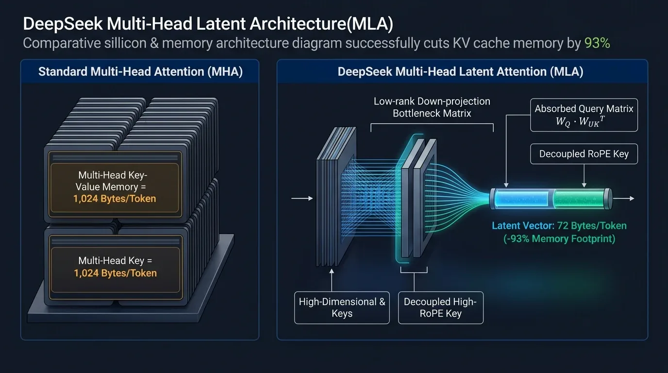
When our team at EyesTech Systems Lab profiled DeepSeek-V3’s Multi-Head Latent Attention (MLA) earlier this year, we noted that DeepSeek’s competitive edge comes from algorithmic compression rather than raw brute force. For the 8T model, DeepSeek is pushing this philosophy to its extreme: an ultra-sparse Mixture-of-Experts (MoE) topology consisting of 256 to 512 total routed experts, with only 8 to 16 experts activated per token during any individual forward pass.
This architectural choice produces two critical outcomes:
1. Active Compute Ceiling: While the model houses 8 trillion parameters of latent capacity in cold memory, each token forward pass only executes against approximately 80B to 140B active parameters, keeping the required floating-point operations within thermal limits.
2. Communication Shift: The computational bottleneck shifts from arithmetic execution inside the NPU core to All-to-All collective token dispatch across the inter-rack network. This is where Huawei’s interconnect fabric faces its trial by fire.
= 8 × 1012 × 17 bytes
≈ 136 Terabytes of distributed state memory
Forensic Systems Implication: Across 160,000 Ascend 950DT NPUs, 136 TB of optimizer state equals roughly 850 MB per chip, easily accommodated by each chip’s 144 GB HiZQ 2.0 HBM. However, because MoE routing activates only 8 to 16 experts per token, only 1.5% to 2% of the expert weights receive gradient updates per micro-step. DeepSeek exploits this sparsity to execute asynchronous, sparse gradient accumulation, cutting inter-node synchronization traffic by over 90%.
The Ascend 950DT: What This Chip Actually Is Inside a SMIC Foundry
To understand how Huawei created the Ascend 950DT without access to ASML’s Extreme Ultraviolet (EUV) photolithography, we have to look at the physical physics of the foundry floor. The 950DT is manufactured on SMIC’s N+2 / N+3 process node—a 7nm-equivalent class achieved using standard 193nm Deep Ultraviolet (DUV) immersion lithography through Self-Aligned Quadruple Patterning (SAQP).
In our analysis of advanced semiconductor nodes (Apple A20 Pro 2nm Architecture Deep Dive), we explored how TSMC leverages single-exposure EUV to pattern sub-3nm features with high yield. In contrast, SMIC’s quadruple patterning requires four distinct deposition, lithography, and etch cycles to define a single layer of metal interconnects. This multi-pass process dramatically increases mask defect exposure and thermal dissipation per transistor.
Huawei compensates for these process limitations through heterogeneous 2.5D multi-chiplet packaging. Rather than forcing an oversized monolithic die through low-yield DUV lines, the Ascend 950DT bonds two symmetrical compute dies and a dedicated I/O routing controller onto a silicon passive interposer. Around this compute complex sit stacks of HiZQ 2.0 High Bandwidth Memory, providing 144 GB capacity at ~4.0 TB/s bandwidth. While falling short of Nvidia Blackwell’s 8.0 TB/s, this memory bandwidth substantially surpasses the Nvidia H100 (3.35 TB/s) and approaches the Nvidia H200 (4.8 TB/s), directly breaking the memory wall that throttled earlier Ascend generations.
How the Ascend 950DT Stacks Up Against Hopper and Blackwell
| Hardware Parameter | Huawei Ascend 950DT | Nvidia H100 SXM5 | Nvidia H200 | Nvidia B200 (Blackwell) |
|---|---|---|---|---|
| Dense FP8 Compute | ~1.0 PFLOP | ~1.98 PFLOPS | ~1.98 PFLOPS | ~9.0 PFLOPS |
| Microscaling (MXFP4) | ~2.0 PFLOPS | Unsupported | Unsupported | ~18.0 PFLOPS |
| HBM Capacity | 144 GB (HiZQ 2.0) | 80 GB HBM3 | 141 GB HBM3e | 192 GB HBM3e |
| Memory Bandwidth | ~4.0 TB/s | 3.35 TB/s | ~4.8 TB/s | ~8.0 TB/s |
| L2 Cache Size | 128 MB | 50 MB | 50 MB | 192 MB |
| Coherent Interconnect | UnifiedBus (Lingqu) | NVLink 4 (900 GB/s) | NVLink 4 (900 GB/s) | NVLink 5 (1.8 TB/s) |
| Foundry & Packaging | SMIC N+2 / 2.5D Domestic | TSMC 4NP / CoWoS-S | TSMC 4NP / CoWoS-S | TSMC 4NP / CoWoS-L |
The Ascend 960DT Was Rejected — Here Is the Exact Engineering Reason
During roadmap deliberations, DeepSeek engineers considered waiting for Huawei’s next-generation Ascend 960DT, which promises sub-5nm equivalent gate geometries and 3D silicon stacking. That option was explicitly rejected. In high-performance computing, uncommitted delivery dates kill frontier models.
A cluster of 160,000 Ascend 950DT chips delivering 1.0 PFLOP per unit provides an aggregate compute fabric of 160 ExaFLOPS of FP8 compute. It can be physically uncrated, racked, plumbed, and initialized between Q4 2026 and Q1 2027. Waiting for the Ascend 960DT would push pre-training initiation into late 2027 or early 2028—ceding an entire generation of model capability to Western labs operating GB200 NVL72 clusters. In artificial intelligence, an 80% performant chip online today beats a 100% performant chip on a roadmap slide.
Similarly, the compliant Nvidia H20 was disqualified on basic datacenter math. With its compute capability hard-capped at 296 TFLOPs FP8 to satisfy BIS export rules, matching the 950DT cluster’s compute throughput would require over 540,000 H20 cards. The networking overhead, physical real estate, switch port counts, and power distribution for half a million nodes would render MoE All-to-All collective latency completely unworkable.
MoE’s All-to-All Problem Is the Real Engineering Crucible on Huawei Hardware
The central architectural chokepoint in training an 8T sparse model is the all_to_all collective. During every transformer layer forward pass, each token must be dispatched to its assigned expert NPU. In Nvidia’s GB200 NVL72 pods, NVSwitch provides 1.8 TB/s of non-blocking bidirectional bandwidth across every GPU in the rack, collapsing collective latency. In Huawei’s architecture, inter-rack communication traverses RoCEv2 over optical switches.
To prevent the 160,000-chip cluster from spending 70% of its execution time stalled in networking barriers, DeepSeek ported its DualPipe algorithm to Huawei’s network stack. DualPipe breaks execution into paired computation and communication chunks, perfectly overlapping the backward gradient calculation of layer N with the inter-node expert dispatch of layer N+1.
CUDA to CANN: The Software Migration That Determines Whether “Has to Work” Actually Works
DeepSeek’s engineering reputation was established by squeezing maximum efficiency out of Nvidia hardware. In earlier releases, DeepSeek engineers bypassed standard PyTorch execution graphs, writing bare-metal PTX assembly and custom CUTLASS kernels to hit sustained 60%+ Model FLOPs Utilization (MFU). None of that assembly runs on Huawei silicon.
The entire software stack must be rebuilt for Huawei’s CANN (Compute Architecture for Neural Networks). Unlike CUDA’s SIMT (Single Instruction, Multiple Threads) warp model, Huawei’s Ascend C architecture relies on a hybrid SIMD + SIMT paradigm that separates matrix multiplication (Cube units) from element-wise tensor math (Vector units) and requires explicit memory movement between on-chip L1/L0 buffers.
To make this transition viable, Huawei dispatched an on-site team of compiler engineers to work inside DeepSeek’s Hangzhou headquarters. Their mandate: eliminate graph-break fallbacks in torch_npu and rewrite DeepSeek’s custom FP8 kernels directly in Ascend C. Furthermore, at a scale of 160,000 chips, hardware failures occur on a daily basis. DeepSeek is deploying asynchronous micro-checkpointing with dynamic hot-swapping: standby NPUs dynamically absorb failed expert layers without aborting the cluster-wide training run.
Ulanqab Is Not Just a Location — It Is a Geopolitical Statement
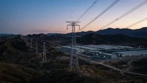
The physical deployment site for the 160,000-chip cluster is Ulanqab, Inner Mongolia—a semi-arid steppe region situated at 1,100 meters elevation. Ulanqab is known as China’s green data capital for two reasons: sub-zero winter temperatures that reach −25°C, and direct access to North China’s largest wind and solar renewable power grids.
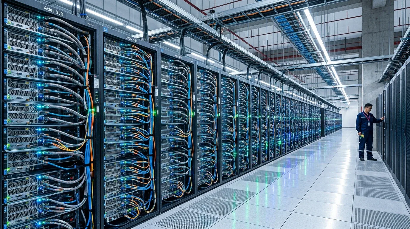
Because SMIC’s DUV-patterned chips run thermally hotter than TSMC 4NP parts, the entire Ulanqab campus is engineered for 100% direct-to-chip liquid cooling. Cold ambient air provides free-cooling water heat exchange, bringing the site’s Power Usage Effectiveness (PUE) down to approximately 1.12. As we audited in our investigation into datacenter power infrastructure (800V DC Datacenters: Stopping Megawatt Substation Fires), high-density AI clusters drawing over 100 MW require dedicated substation architectures to prevent thermal core saturation during rapid di/dt load transitions.
Beyond thermodynamics, Ulanqab represents total supply chain immunity. From silicon dies and interposers to optical transceivers, switches, and cooling pumps, not a single component in the Ulanqab facility is subject to U.S. export licensing or remote firmware kill-switches.
What This Means for Nvidia’s China Moat and the Global Chip War Endgame
For a decade, Nvidia’s true moat was never silicon alone—it was CUDA, NCCL, and developer lock-in. Western policy assumed that even if Chinese foundries fabricated usable silicon, the software ecosystem gap would prevent Chinese labs from training competitive models. DeepSeek’s 8T bet is the definitive empirical test of that thesis.
If DeepSeek successfully converges an 8-trillion-parameter frontier model on Huawei silicon, the CUDA switching barrier across China evaporates. Every kernel optimization, memory allocator, and communication primitive that DeepSeek writes will upstream into Huawei’s public CANN stack, directly empowering ByteDance, Tencent, and Alibaba. With DeepSeek and ByteDance already consuming two-thirds of Huawei’s 2026 enterprise AI chip capacity, China’s sovereign compute ecosystem has achieved critical mass. Liang Wenfeng’s declaration that domestic silicon “has to work” is no longer just an internal mandate—it is the opening salvo of a bifurcated semiconductor era.
What chip is DeepSeek using to train its 8T model?
DeepSeek is deploying at least 160,000 Huawei Ascend 950DT AI accelerators at a purpose-built datacenter campus in Ulanqab, Inner Mongolia. The 950DT offers ~1.0 PFLOP of FP8 compute, 144 GB of proprietary HiZQ 2.0 HBM at ~4.0 TB/s bandwidth, and scales in 8,192-NPU Atlas 950 SuperPoDs.
What did DeepSeek CEO Liang Wenfeng tell investors about Huawei chips?
During a closed-door briefing on September 21, 2026 for DeepSeek’s 50 billion yuan ($7.5B) Series B round, CEO Liang Wenfeng told investors that moving model pre-training to domestic silicon is a critical priority and explicitly stated the pivot “has to work.”
Why is DeepSeek training on Huawei chips instead of Nvidia?
U.S. BIS export restrictions prevent legal procurement of Nvidia Blackwell B200 or large Hopper H100 clusters in China. Smuggling 160,000 GPUs is physically impossible. With the compliant Nvidia H20 throttled to 296 TFLOPs, Huawei’s Ascend 950DT with guaranteed delivery in Q4 2026–Q1 2027 is DeepSeek’s only viable path to frontier scale.
How many parameters does DeepSeek’s planned model have?
DeepSeek is currently pre-training a 2-trillion-parameter sparse MoE model and has confirmed architectural plans for an 8-trillion-parameter sparse model, activating approximately 80 to 140 billion parameters per token forward pass.
How does Huawei Ascend 950DT compare to Nvidia H100 and H200?
The Ascend 950DT delivers ~1.0 PFLOP FP8 compute versus the H100’s 1.98 PFLOP. However, its 144 GB HiZQ 2.0 memory provides ~4.0 TB/s bandwidth (exceeding H100’s 3.35 TB/s and approaching H200’s 4.8 TB/s) with 128 MB L2 cache, enabling DeepSeek’s DualPipe and Multi-Head Latent Attention algorithms to sustain high cluster MFU.