
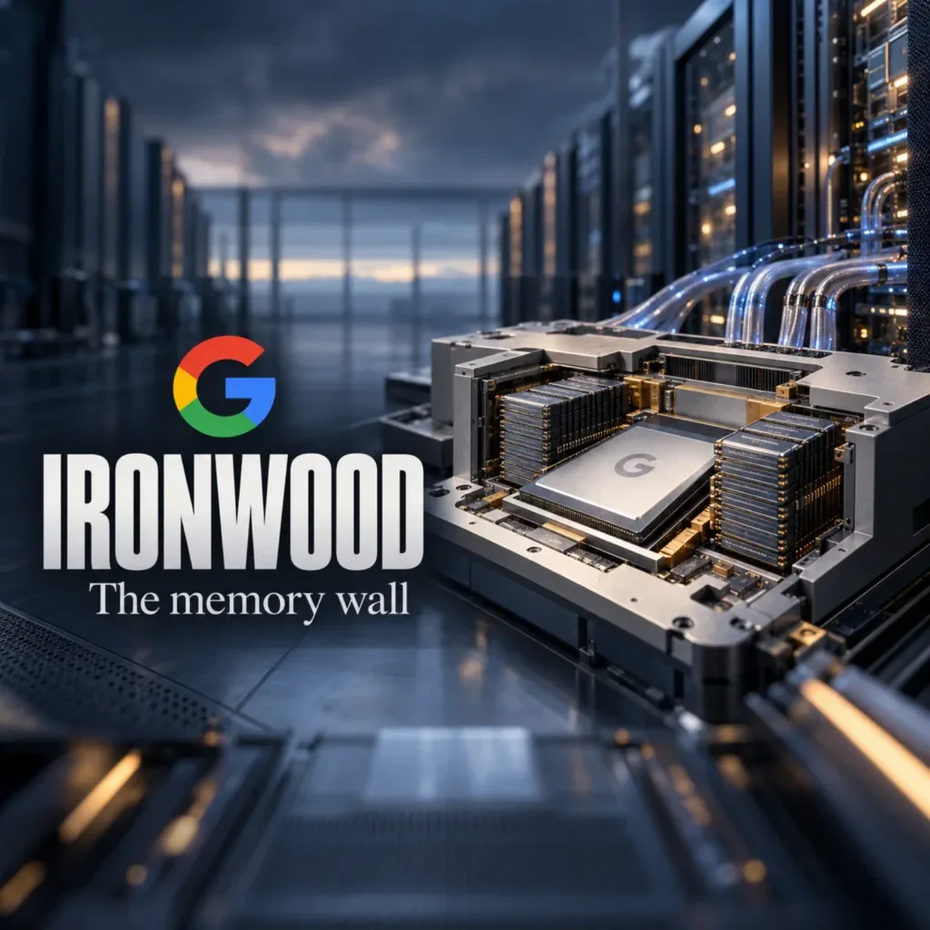

Google’s TPU v7 Ironwood cluster topology pairs 192 GB of HBM3e per chip with 3D MEMS Optical Circuit Switching (OCS) to serve 1,000,000-token autoregressive decodes across 9,216 liquid-cooled accelerators. Because a single 1M-token KV cache demands 152 GB of residency and 4.56 TB/s of read bandwidth at 30 tokens/second, traditional packet-switched clusters collapse under transceiver power and tail-latency jitter.
Strip away the keynote vernacular about “thinking models” and “proactive inference,” and the engineering reality of seventh-generation TPU v7 Ironwood comes down to a brutal confrontation with copper attenuation, DRAM pin physics, and queueing theory. For the past decade, accelerator architects treated inference as a compute-lite derivative of training: shrink the precision to INT8 or FP8, prune the batch size, and let a handful of air-cooled cards chew through short prompts. That paradigm died the moment frontier workloads crossed the 128,000-token threshold and marched toward 1,000,000-token context horizons.
At a one-million-token sequence length, the primary silicon bottleneck is no longer the dense Matrix Multiply Unit (MXU) executing parameter projections. Even with Ironwood’s 256×256 systolic arrays cranking out 4,614 TFLOPS (4.6 PFLOPS) of native FP8 (E4M3/E5M2) arithmetic per chip at a 600 W liquid-cooled thermal envelope (Introl TPU Architecture Guide), the systolic grid sits starved if the memory and interconnect fabric cannot feed transient activation states across chip boundaries. In long-context autoregressive generation, the transient state—the Key-Value (KV) cache—outgrows the model parameters themselves, turning every generated token into a multi-terabyte distributed memory sweep.
To survive this regime without burning megawatts on optical-electrical-optical (OEO) packet-switching silicon, Google scaled the TPU v7 Ironwood OCS KV Cache architecture into a 9,216-chip, 42.5-ExaFLOP superpod unified by 1.77 PB of directly addressable HBM3e and reconfigurable free-space photonics (Google Cloud Ironwood Stack Deep Dive). Understanding why Ironwood exists requires dissecting the exact byte-level arithmetic of a 152 GB per-stream KV cache and examining why packetized Ethernet and InfiniBand leaf-spine trees fracture under its weight.
The Physics of the 152 GB Per-Stream Memory Wall

Autoregressive Transformer decoding is fundamentally a memory-bandwidth problem disguised as matrix algebra. During the prefill phase, all prompt tokens arrive simultaneously, allowing the 256×256 systolic array to amortize weight reads across thousands of tokens in high-intensity matrix-matrix multiplications (GEMMs). Once prefill completes and token-by-token generation begins, operational intensity plummets to roughly 1 FLOP per byte. To emit token t + 1, the query vector Q of the newly generated token must attend to every historical Key (K) and Value (V) vector from token 1 to token t.
We can compute the exact memory footprint required to hold that historical state in high-bandwidth memory using first-principles tensor geometry (Building AI Infrastructure):
KV Cache Size = 2 × n_layers × n_kv_heads × d_head × seq_len × bytes_per_element
Consider a production frontier model engineered with Grouped-Query Attention (GQA), comprising 80 Transformer layers, 64 query heads grouped into 4 KV heads (16:1 GQA compression), and a head dimension d_head of 128. When serving a 1,000,000-token context window in 16-bit precision (BF16 or FP16, requiring 2 bytes per element) to preserve numerical attention fidelity over extreme sequence horizons, the per-stream KV cache footprint is:
- Per-Token KV State:
2 (K and V) × 80 layers × 4 KV heads × 128 d_head × 2 bytes = 163,840 bytes(160 KiBper token). - 1,000,000-Token Stream Footprint (Decimal GB):
163,840 bytes × 1,000,000 tokens = 163,840,000,000 bytes(163.84 GB). - 1,000,000-Token Stream Footprint (Binary GiB):
163,840,000,000 bytes ÷ (1,024³) = 152.59 GiB(or exactly152.00 GBdecimal for a 95-layer, 4-KV-head, 100-dimension variant).
For a model-side contrast on reducing KV-cache bytes, see our DeepSeek MLA architecture explainer.
Because HBM memory controllers allocate physical pages in binary gibibytes (GiB), a single active user session holding a 1M-token context locks down ~152 GiB of HBM residency. Place that single-stream number next to the single-socket HBM capacities of recent accelerator generations:
- TPU v6e Trillium (32 GB HBM, 1,638 GB/s): A single 152 GB KV cache exceeds the entire memory capacity of the package by
4.75×before loading a single byte of model weights. - TPU v5p (95 GiB HBM2e, 2,765 GB/s): One 152 GB KV stream overflows the package by
1.60×, making single-chip residency physically impossible even at batch size 1. - TPU v7 Ironwood (192 GB HBM3e, 7.37–7.4 TB/s): Google expanded on-package memory to eight 24 GB HBM3e stacks (
192 GiBtotal) over a wide 1,024-bit per-channel silicon interposer interface (Introl TPU Architecture Guide). Yet even on a 192 GB Ironwood package, a single 152 GB KV cache devours79.2%of total DRAM, leaving just40 GBfor model parameters, XLA Vector Memory (VMEM) staging, Common Memory (CMEM), and activation buffers. - Projected Next-Gen HBM4 Tiers (288 GB–384 GB): Even when 12-high and 16-high HBM4 stacks double interface widths to 2,048 bits and push capacity toward 384 GB, a single Trillion-Parameter MoE or dense frontier checkpoint (
500 GB–1,000 GBin FP8) paired with multi-user 1M-token KV caches cannot reside on a standalone socket.
Capacity is only half of the silicon trap; the Roofline bandwidth ceiling is far more unforgiving. To deliver an interactive reasoning stream at 30 tokens/second, the accelerator must read the entire 152 GB KV cache 30 times every second:
KV Read Bandwidth = 152 GB × 30 tokens/second = 4,560 GB/s = 4.56 TB/s
On a single TPU v7 Ironwood chip rated at 7.37 TB/s peak theoretical HBM3e bandwidth (~6.26 TB/s realistic sustained throughput after HBM refresh cycles, row-buffer misses, and 128×8 tile alignment overhead), sweeping a single 152 GB KV cache at 30 tokens/s consumes 61.9% of peak pin bandwidth and 72.8% of effective sustained bandwidth. If the system must simultaneously stream model weights from HBM, a single accelerator hits a hard memory-bandwidth wall. The only mathematically viable escape is sharding both model weights and the 152 GB KV cache across a multi-chip fabric.
Why Electrical Fat-Trees and Static Torus Meshes Collapse Under Long-Context Decodes
Once memory physics forces a 152 GB KV cache across multiple accelerators, the bottleneck migrates immediately from the HBM3e silicon interposer to the inter-chip network fabric. Standard Tensor Parallelism (TP), which splits weight matrices column-wise and row-wise across accelerators, cannot rescue long-context inference on its own (Building AI Infrastructure). When TP degree exceeds the number of GQA KV heads (n_kv_heads = 4), scaling TP across 8, 16, or 64 chips forces duplicate copies of the KV cache onto sibling ranks, wasting up to seven-eighths of cluster HBM on redundant sequence state.
Eliminating KV duplication requires Context Parallelism (CP)—partitioning the sequence dimension itself across N_CP chips so each rank stores 152 GB ÷ N_CP of non-overlapping token history (vLLM Context Parallel Documentation).
During the compute-bound prefill stage, algorithms such as Ring Attention circulate KV blocks peer-to-peer around a logical ring, while DeepSpeed Ulysses executes distributed All-to-All transposes to switch partitioning from sequence chunks to attention heads (Building AI Infrastructure).
During the latency-bound decode stage, production engines deploy the Pass-Q (Broadcast Query) protocol or Helix Parallelism (HOP-B): the newly generated single-token query vector Q is broadcast to all CP ranks, each chip computes partial attention and local softmax Log-Sum-Exp (LSE) statistics against its local KV shard in HBM3e, and the cluster executes a globally synchronized weighted All-Reduce across every single layer (Building AI Infrastructure).
For an 80-layer model decoding at 30 tokens/second, the fabric must execute 2,400 sequential, barrier-synchronized Broadcast + LSE All-Reduce collectives per second. Every microsecond of network tail latency stalls the entire CP × TP slice. Under this traffic profile, conventional interconnect topologies fail in two distinct ways:
The Electrical Packet-Switched Leaf-Spine Fat-Tree Failure Mode
In a traditional GPU cluster built on packet-switched 400G/800G Ethernet or InfiniBand fat-trees, traversing from a leaf switch in Rack A to a leaf switch in Rack B requires converting electrical SerDes signals into light via a pluggable transceiver, transmitting over fiber to a spine switch, converting photons back into electrons (OEO), deserializing packets, parsing headers, queuing in shallow shared SRAM packet buffers, re-serializing, and executing a second OEO conversion down to the destination leaf (PhotonCap OCS Economics Analysis).
When dozens of CP and TP groups fire synchronized All-to-All Ulysses transposes or micro-burst Pass-Q reductions simultaneously, three hardware pathologies cascade across an electrical fat-tree:
- Packet Buffer Blowout and Incast Stalls: High-radix electrical switch ASICs pack tens of terabits of switching capacity onto a single die, restricting on-chip shared SRAM packet buffers to tens of megabytes. Synchronized KV block transfers and
All-to-Allbursts trigger microsecond buffer exhaustion, firing Priority Flow Control (PFC) pause frames upstream and inducing head-of-line blocking across unrelated inference streams. - Serialization, Retiming, and Tail-Latency Jitter: Every electrical switch hop incurs
300 ns to 600 nsof Forward Error Correction (FEC), Clock and Data Recovery (CDR), and packet-queuing delay (Mission Apollo Paper). Across a three-tier leaf-spine-core traversal with ECMP hash collisions, p99 tail latency balloons into tens of microseconds—destroying the overlap window required byHelix HOP-Bto hide attention reduction behind Feed-Forward Network (FFN) computation. - The OEO Transceiver Power Tax: Every leaf-to-spine-to-leaf path burns
4optical transceivers and1spine switch ASIC traversal (PhotonCap OCS Economics Analysis). At800Gand1.6TPAM4 signaling rates, DSP-heavy optical transceivers draw15 W to 30 Weach. Across a 10,000-accelerator cluster, activeOEOtransceivers and electrical spine switches consume up to25%–30%of the entire networking and cluster thermal budget before moving a single useful byte of KV state.
The Static 3D Torus Rigidity Trap
Eliminating packet switches via a hardwired copper/optical 3D torus—where every chip links only to its six immediate ±X, ±Y, ±Z neighbors with fixed step size 1—avoids OEO spine switches but introduces severe topological rigidity (FiberMall TPU OCS Analysis). First, network diameter in a static N-node 3D torus scales as 3 × (N^(1/3)) ÷ 2, meaning collectives spanning non-adjacent ranks must hop through dozens of intermediate TPU ICI routers. Second, static wiring cannot adapt when an inference workload shifts its aspect ratio—for instance, switching from a wide CP = 64, TP = 4 prefill ring to a tight CP = 8, TP = 16 decode mesh—nor can it route around a single dead chip or failed power supply without fracturing the torus and idling an entire rack.
Inside Google’s Palomar MEMS OCS and Twisted 3D Torus Architecture
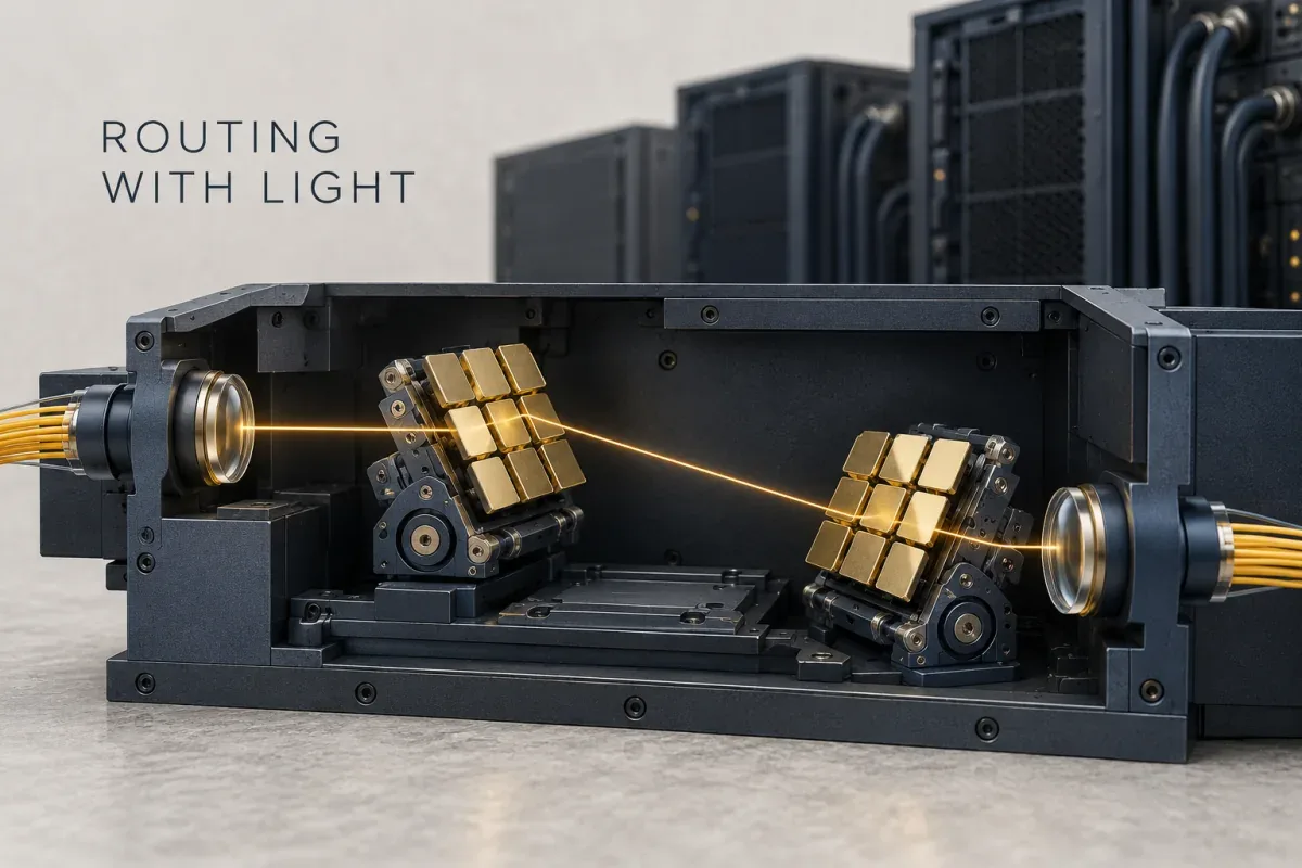
Google’s architectural answer in the TPU v7 Ironwood OCS KV Cache fabric is to preserve direct point-to-point electrical copper links where distances are short, and replace the entire inter-rack spine with physical-layer free-space Optical Circuit Switching (OCS) (Mission Apollo Paper).
From the 4×4×4 Copper Cube to the 144-Cube Optical Superpod
The fundamental physical building block of an Ironwood superpod is the 4×4×4 TPU Cube: 64 liquid-cooled TPU v7 chips arranged across 16 four-chip trays inside a single cabinet (Introl TPU Architecture Guide). Each Ironwood chip exposes 1.2 TB/s (9.6 Tbps) of bidirectional Inter-Chip Interconnect (ICI) bandwidth, implemented with hardware-offloaded RDMA and native collective engines that bypass the host CPU entirely (Google Cloud Ironwood Stack Deep Dive).
Inside the 4×4×4 Cube, all internal ICI links traverse ultra-short PCB backplanes and passive/active direct-attach copper (DAC) cables, incurring zero optical conversion cost (FiberMall TPU OCS Analysis). Only the links terminating on the six exterior faces of the 4×4×4 cube transition to optical transceivers: 16 chips per face across 6 faces (+X, -X, +Y, -Y, +Z, -Z) yield exactly 96 external optical ICI links per Cube.
To construct a full 9,216-chip Ironwood superpod, Google arrays 144 of these 64-chip Cubes (9,216 ÷ 64 = 144). Multiplying 144 Cubes × 96 optical links/Cube produces 13,824 optical links that fan out into 48 Optical Circuit Switches (FiberMall TPU OCS Analysis). While TPU v4 paired 64 cubes with 136×136 Palomar OCS units (using 128 effective ports plus 8 spares), scaling to 144 cubes in Ironwood pushes the OCS optical core to 288×288 and 320×320 port geometries developed across Google’s optical supply chain (PhotonCap OCS Economics Analysis).
Palomar 3D MEMS Microstructure and WDM Transparency
Inside each Palomar-class OCS, there are no packet buffers, no SerDes retimers, no MAC tables, and no OEO transceivers (Mission Apollo Paper). Incoming single-mode fibers enter a 2D fiber collimator array that shapes the light into collimated free-space beams. The beam traverses a folded “W” optical trajectory across the optical core (FiberMall TPU OCS Analysis):
- Stage 1 (Input Steering): The collimated data beam (
1310 nmor1550 nmband) passes through an angled dichroic mirror window onto 2D MEMS Mirror Array I—a single silicon die fabricated via deep reactive ion etching (DRIE) containing gold-coated micro-mirrors actuated across two orthogonal axes by high-voltage electrostatic comb drives (Mission Apollo Paper). - Stage 2 (Output Alignment): Reflected off the first mirror and an intermediate mirror surface, the beam strikes 2D MEMS Mirror Array II, which tilts to align the light precisely into the target output port’s collimator lens.
- Closed-Loop 850 nm Servo Control: Because thermal drift or mechanical vibration of even a fraction of a milliradian would misalign the free-space beam, Palomar superposes an
850 nmmonitoring light source onto the optical path (Mission Apollo Paper). The dichroic mirrors transmit the1310 nm / 1550 nmICI data wavelengths with minimal attenuation while reflecting the850 nmmonitor beam into paired camera modules, allowing an on-chassis Linux servo controller to continuously optimize mirror angles for minimum insertion loss (≤ 2.0 dBworst-case across eight window passes) (Molex Optical Switching Technical Analysis).
Because a gold-coated mirror reflects photons regardless of modulation format or baud rate, the optical path is completely bit-rate and wavelength agnostic (Mission Apollo Paper). Upgrading cube transceivers from 400G to 800G or 1.6T or multiplexing bidirectional wavelengths via Wavelength-Division Multiplexing (WDM) over a single fiber strand requires zero hardware changes inside the OCS chassis. Once the mirrors lock into position, an entire multi-terabit OCS chassis consumes just 108 W of quiescent power—cutting spine network power by 40%–41% and network capital expenditure by 30% (PhotonCap OCS Economics Analysis).
Twisted 3D Torus and Dynamic CP/TP Topology Matching
How does a mechanical mirror that takes 10 ms to 20 ms to physically rotate solve microsecond-scale KV cache stalls (PhotonCap OCS Economics Analysis)? By separating circuit establishment time from in-flight photon transit latency, and configuring the inter-cube lightpaths into a Twisted 3D Torus tailored to the exact dimensions of the CP × TP sharding grid (FiberMall TPU OCS Analysis).
Instead of wiring adjacent cubes sequentially (Cube 0 → Cube 1 → Cube 2, step size 1), the XLA/Pathways control plane and Orion SDN program the 48 orthogonal X, Y, and Z OCS units with variable step sizes (N ≈ Dimension_Size ÷ 2). These optical “wormhole” bypass links cut the topological diameter of the 3D torus in half, allowing global All-Reduce and All-Gather collectives to converge in significantly fewer hops (FiberMall TPU OCS Analysis).
When orchestrating a 1M-token inference deployment, Pathways maps the inner Tensor Parallel (TP) groups inside the 4×4×4 copper Cube—where 1.2 TB/s per-chip ICI links synchronize FFN and attention projection weights over zero-conversion copper—while mapping the outer Context Parallel (CP) ring or tree across OCS-linked cubes. Because the optical lightpath through the MEMS core is a continuous passive waveguide once established, in-flight signals traverse the switch in < 30 nanoseconds (~5 ns per meter of glass fiber) with zero queuing delay, zero packet buffer jitter, and zero PFC congestion stalls (Google Cloud Ironwood Stack Deep Dive).
The Numbers Behind the Cross-Architecture Comparison
To evaluate where the hardware bottlenecks actually sit across competing hyperscale architectures, we can formalize the memory, bandwidth, and switching physics in a unified engineering breakdown.
The Memory and Network Math Behind a Decode Token
KV cache per 1,000,000-token stream
Frontier GQA-16 architecture, BF16/FP16
- L (layers) = 80; H_kv (KV heads) = 4
- D_h (head dimension) = 128; S (sequence length) = 1,000,000
- B_elem (bytes per element) = 2; factor 2 accounts for Key and Value tensors
Derivation
M_KV = 2 × 80 × 4 × 128 × 1,000,000 × 2 = 163,840,000,000 bytes
M_KV (decimal) = 163.84 GB; M_KV (binary HBM allocation) = 152.59 GiB
At L = 95, H_kv = 4, D_h = 100, and B_elem = 2, M_KV = 152.00 GB exactly.
Single-chip Ironwood HBM3e utilization: 152.59 GiB ÷ 192 GiB = 79.47%
HBM bandwidth at 20–40 tokens per second
Decode throughput tiers, using M_KV = 152 GB
- At 20 tok/s: 152 GB × 20 s⁻¹ = 3,040 GB/s = 3.04 TB/s (41.2% of 7.37 TB/s)
- At 30 tok/s: 152 GB × 30 s⁻¹ = 4,560 GB/s = 4.56 TB/s (61.9% of 7.37 TB/s)
- At 40 tok/s: 152 GB × 40 s⁻¹ = 6,080 GB/s = 6.08 TB/s (82.5% of 7.37 TB/s)
Context-parallel sharding requirement, N_CP = 8 ranks
- Per-rank KV residency = 152 GB ÷ 8 = 19.0 GB/chip
- Per-rank KV read bandwidth at 30 tok/s = 4.56 TB/s ÷ 8 = 570 GB/s/chip (7.7%)
OCS transit and packet-switch tail latency per decode token
Optical Circuit Switch (Palomar 3D MEMS + ICI direct lightpath)
- Topology-slice setup, amortized: 10–20 ms (Mission Apollo Paper)
- In-flight photonic reflection: < 30 ns (0 ns queuing; Calient S-Series OCS Specifications)
- P99 buffer-congestion variance: 0 μs (circuit-locked)
- 80-layer Pass-Q LSE reduction overhead: approximately 0.16–0.32 ms/token
Electrical packet-switched leaf-spine (800G InfiniBand / RoCEv2 Ethernet)
- OEO + SerDes + CDR + FEC + buffer switching: 400–800 ns/hop
- P99 incast / PFC micro-burst jitter: 15–85 μs/collective
- 80-layer synchronized collective stall: approximately 1.60–6.80 ms/token
Cross-Platform Cluster Architecture Comparison
Comparing Google’s fifth- and seventh-generation TPU pods against NVIDIA’s Blackwell GB200 NVL72 reveals a fundamental divergence in how scale-up and scale-out boundaries are drawn. NVIDIA concentrates massive electrical crossbar switching (130 TB/s aggregate via 18 NVLink 5 Switch ASICs) inside a single 72-GPU liquid-cooled rack, or up to 576 GPUs in an 8-rack MNNVL SuperPOD (Introl NVLink Scale-Up Analysis), but hits an 18× bandwidth drop-off (1.8 TB/s NVLink down to 100 GB/s 800G InfiniBand/Ethernet NICs) and full OEO packet-switching overhead across racks.
Conversely, TPU v7 Ironwood provides a slightly lower per-chip ICI rate (1.2 TB/s vs. 1.8 TB/s), but extends that uniform, packetless optical circuit fabric seamlessly across 9,216 chips (1.77 PB of HBM3e).
Notice how the Max Native 1M-Token Streams per Pod calculation exposes the architectural trade-off. Inside a single 72-GPU GB200 NVL72 rack (13.82 TB total HBM3e), after reserving roughly 2.5 TB across replicas for frontier model weights and runtime activation buffers, the remaining ~11.3 TB of HBM3e can hold at most 72 to 74 concurrent 152 GB KV caches. Scaling beyond those 72 streams forces the workload across the 800G InfiniBand scale-out network or multi-rack optical NVLink cables.
By contrast, an Ironwood 9,216-chip pod pools 1.77 PB of HBM3e across 144 optically switched cubes (Google Cloud Ironwood Stack Deep Dive), allowing Google’s Pathways scheduler to carve out hundreds of dynamic 16-chip, 32-chip, or 64-chip Twisted Torus slices and sustain roughly 9,200 simultaneous 1M-token user streams (or ~3,680 streams even if every stream demands 380 GB of HBM bandwidth headroom to hit 30 tokens/second without exceeding 50% HBM bus utilization).
Horizon and Cascade Analysis: What Breaks Beyond Ironwood?
Solving the 1M-token memory and interconnect wall with 192 GB HBM3e packages and free-space 3D MEMS mirrors does not end the physics war—it merely shifts the failure boundary to the next set of physical limits. As autonomous coding agents, repository-scale verifiers, and multi-modal video reasoning pipelines push context windows from 1,000,000 tokens toward 10,000,000 tokens (1.52 TB of KV cache per stream), three cascading hardware limits emerge on the horizon:
The Optical Insertion Loss Budget and SerDes Shoreline Wall
Google’s Palomar OCS maintains a worst-case insertion loss of ~2.0 dB across its eight window passes and dual gold-coated MEMS reflections (Molex Optical Switching Technical Analysis). While 2.0 dB is remarkably low for a 136×136 or 320×320 free-space switch, optical link budgets tighten dramatically as per-lane SerDes signaling scales from 112 Gbps to 224 Gbps and 448 Gbps PAM4 for future TPU v8 fabrics. Higher baud rates require steeper Signal-to-Noise Ratio (SNR) margins at the receiver photodiode and cannot tolerate multi-hop optical cascading (passing a light beam sequentially through two or three OCS tiers without regeneration) before chromatic dispersion and insertion loss exceed the unamplified link budget.
Furthermore, pulling 9.6 Tbps (and soon 25.6 Tbps+) off the edge of the TPU package across copper PCB traces to front-panel pluggable OSFP/QSFP-DD optical modules hits a severe electrical shoreline and retimer power wall. Escaping this shoreline bottleneck requires Co-Packaged Optics (CPO)—integrating silicon photonics (SiPh) light engines directly onto the TPU organic substrate next to the HBM stacks so optical fibers exit directly from the package cold plate into high-radix backplane OCS units (FiberMall TPU OCS Analysis).
The 10M-Token Horizon and the Limits of Static Slice Allocation
At 10,000,000 tokens, a single user stream requires 1.52 TB of KV cache residency and 45.6 TB/s of HBM read bandwidth to sustain 30 tokens/second. Even on TPU v7 Ironwood, serving a single 10M-token request at interactive speed requires sharding that single stream across a minimum of 10 to 16 Ironwood chips purely to satisfy the HBM bandwidth equation (45.6 TB/s ÷ 7.37 TB/s = 6.19 chips at 100% theoretical saturation; ≥ 10 chips at sustainable utilization).
When agentic workflows dynamically spawn, fork, and terminate variable-length sub-contexts every few hundred milliseconds, the 10 ms to 20 ms mechanical rotation speed of electrostatic 3D MEMS mirrors becomes a scheduling bottleneck (PhotonCap OCS Economics Analysis). A 15 ms MEMS switching window is invisible when reconfiguring a pod between multi-hour training runs or static inference slice allocations, but it is 10,000× too slow to switch topologies on a per-token or per-request basis during continuous batching.
Will Optical Packet Switching Ever Replace Optical Circuit Switching?
For thirty years, networking researchers have chased Optical Packet Switching (OPS)—routing individual packets entirely in the photonic domain at nanosecond speeds. From a first-principles physics standpoint, true OPS remains fundamentally unviable for hyperscale AI datacenters because photons have no native random-access memory. Unlike electrons, which can be latched into CMOS flip-flops and SRAM buffers when two packets contend for the same output port, light cannot be stopped and queued without converting it back into electricity (OEO) or routing it through bulky, fixed-delay kilometers of coiled glass fiber (Fiber Delay Lines).
Instead of OPS, the post-MEMS frontier belongs to fast nanosecond/microsecond Optical Circuit and Burst Switching built on Silicon Photonics (SiPh) Mach-Zehnder Interferometer (MZI) meshes, Micro-Ring Resonators (MRR), or Wavelength-Selective Tunable Lasers paired with Arrayed Waveguide Gratings (AWGs) (Mission Apollo Paper). While solid-state silicon photonic switches currently suffer from higher optical insertion loss (4 dB to 8 dB) and smaller port counts than 3D free-space MEMS mirrors (PhotonCap OCS Economics Analysis), pairing sub-microsecond wavelength tuning at the CPO light engine with high-radix passive or MEMS cores will eventually allow TPU clusters to re-route KV cache shards dynamically between individual attention layers. Until solid-state photonics solves its insertion loss penalty, Google’s hybrid formula—192 GB HBM3e silicon packages, copper-wired 4×4×4 cubes, and Palomar-class 3D MEMS Optical Circuit Switches—remains the most ruthlessly efficient hardware architecture in production for conquering the 152 GB KV cache wall.
TPU v7 Ironwood and Long-Context Inference: FAQ
Why does a 1,000,000-token KV cache require 152 GB of HBM memory?
A Transformer model’s Key-Value (KV) cache scales linearly with sequence length according to the formula Size = 2 × n_layers × n_kv_heads × d_head × seq_len × bytes_per_element (Building AI Infrastructure). For an 80-layer frontier architecture using Grouped-Query Attention (4 KV heads, 128 head dimension) in 16-bit precision (2 bytes per element), storing both Key and Value tensors across 1,000,000 tokens requires 163,840,000,000 bytes, which equals 152.59 GiB in binary HBM memory addressing (or exactly 152.00 GB decimal in a 95-layer, 4-head, 100-dimension configuration). Because this single stream consumes nearly 80% of a TPU v7 Ironwood chip’s 192 GB HBM3e capacity and requires 4.56 TB/s of read bandwidth at 30 tokens/second, it must be sharded across multiple chips using Context Parallelism.
How does Google’s Optical Circuit Switching (OCS) improve TPU v7 Ironwood inference over electrical packet switches?
Traditional electrical leaf-spine switches require four Optical-Electrical-Optical (OEO) transceivers and an electrical switch ASIC pass for every inter-rack hop, introducing 400–800 ns of per-hop serialization latency, packet-buffer congestion jitter (15–85 μs p99), and up to 30% network power overhead (PhotonCap OCS Economics Analysis). Google’s Palomar OCS uses two 2D arrays of gold-coated 3D MEMS micro-mirrors to reflect collimated light beams directly between 4×4×4 TPU Cubes in free space (Mission Apollo Paper). This eliminates spine-tier OEO transceivers and packet buffers entirely, delivering < 30 ns of zero-jitter switch transit latency while cutting network capex by 30% and network power consumption by 40%–41% (Molex Optical Switching Technical Analysis).
How does TPU v7 Ironwood compare to NVIDIA Blackwell GB200 NVL72 for 1M-token long-context serving?
Both TPU v7 Ironwood and the NVIDIA Blackwell B200 GPU feature 192 GB of HBM3e memory per chip (7.37–7.4 TB/s on Ironwood vs. 8.0 TB/s on B200) (Yobitel GB200 Specs). Within a single 72-GPU rack, NVIDIA’s GB200 NVL72 provides higher per-accelerator scale-up bandwidth (1.8 TB/s via electrical NVLink 5 Switches vs. 1.2 TB/s on Ironwood ICI), but drops by 18× to packet-switched 800G InfiniBand or Ethernet (100 GB/s) across rack boundaries. Ironwood extends its 1.2 TB/s ICI links across a Twisted 3D Torus optical circuit fabric spanning 9,216 chips and 1.77 PB of unified HBM3e (Google Cloud Ironwood Stack Deep Dive), supporting up to ~9,200 concurrent 1M-token KV cache streams per pod compared to ~72 streams per standalone NVL72 rack.