
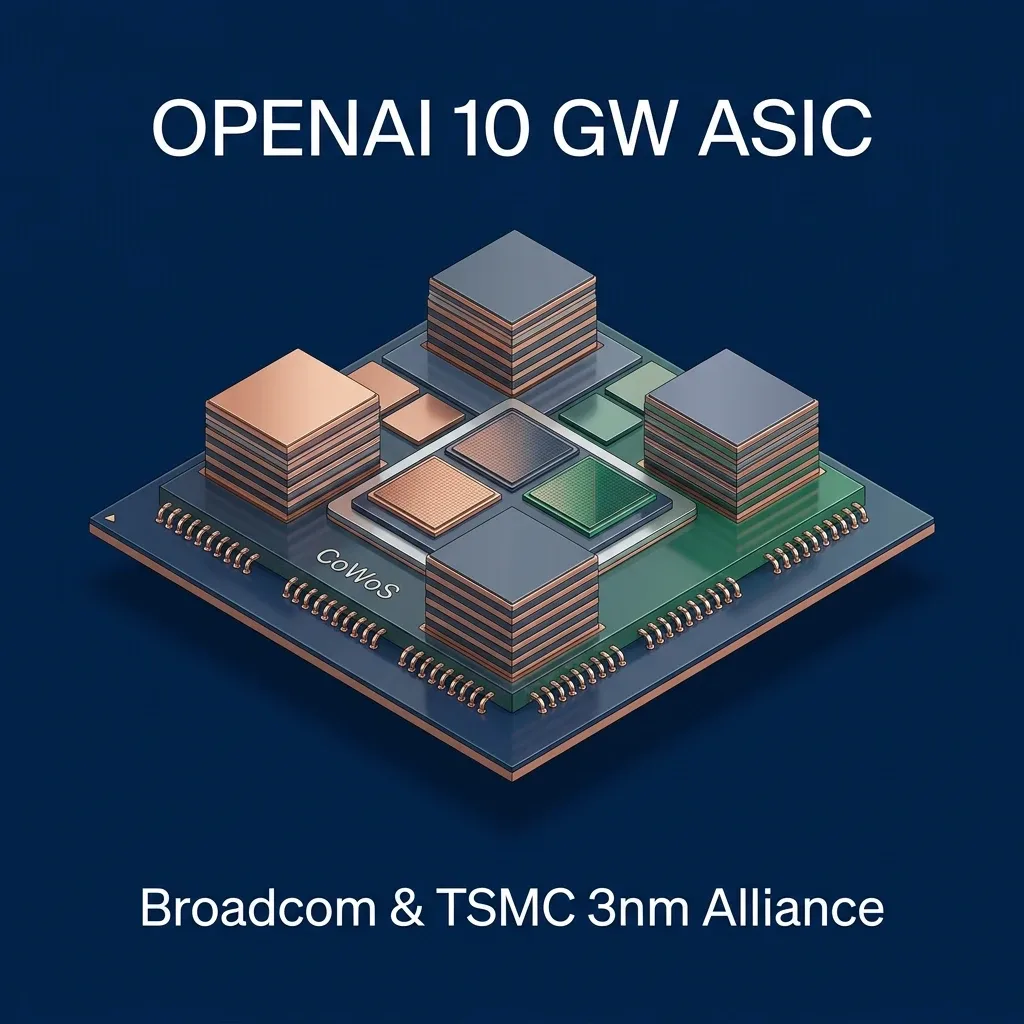

OpenAI has partnered with Broadcom and TSMC to co-design and deploy 10 gigawatts of custom AI inference processors through 2029, securing advanced 3nm and 2nm foundry allocations, integrating Broadcom Tomahawk 5 Ethernet networking, and aiming to reduce per-token inference serving costs by 55% to 65% compared to commercial Nvidia GB200 systems.
The Co-Design Blueprint: TSMC 3nm Silicon and CoWoS Packaging
The architectural details of OpenAI’s custom silicon program, reported by The Information and corroborated through supply-chain reporting in TechCrunch, dismantle Sam Altman’s earlier $7 trillion foundry ambition in favor of a pragmatic fabless co-design model. Rather than attempting to finance and build greenfield semiconductor fabrication facilities, OpenAI formed an engineering alliance with Broadcom, contracting Taiwan Semiconductor Manufacturing Company (TSMC) for direct foundry execution.
The initial processor family is scheduled for physical tape-out on TSMC’s N3P (3-nanometer performance-enhanced) and subsequent N2 (2-nanometer gate-all-around nanosheet) nodes. The internal hardware division is led by former Google TPU engineering architects Richard Ho and Thomas Norrie, who have scaled OpenAI’s internal hardware engineering unit to over 40 ASIC designers and physical packaging specialists.
Crucially, the physical throughput limiter of modern AI accelerator production does not reside purely in front-end wafer fabrication; it is constrained by advanced back-end packaging. OpenAI and Broadcom have reserved dedicated allocation on TSMC’s Chip-on-Wafer-on-Substrate with Local Silicon Interconnect (CoWoS-L) packaging lines. CoWoS-L utilizes organic substrates embedded with passive silicon bridges, enabling multi-die packaging alongside dense high-bandwidth memory (HBM3e and next-generation HBM4) stacks without the yield penalties associated with monolithic full-reticle silicon. Similar to Alibaba’s 20GW Zhenwu V900 deployment, custom packaging has become the true determinant of AI compute sovereignty.
| Packaging Parameter | Nvidia Blackwell B200 | OpenAI / Broadcom ASIC Gen-1 | Physical Advantage |
|---|---|---|---|
| Silicon Lithography Node | TSMC 4NP (Custom 5nm class) | TSMC N3P (3nm EUV) | ~1.30× logic density; 18% lower dynamic power |
| Packaging Architecture | Dual-die CoWoS-L (10 TB/s bridge) | Custom Multi-Die CoWoS-L | Tailored SRAM-to-compute ratio; optimized thermal profiles |
| Target Workload Profile | Unified Training & Inference | Dedicated Autoregressive Inference | Zero silicon area wasted on FP64 or unneeded matrix pipelines |
| Interconnect Standard | Proprietary NVLink 5 (1.8 TB/s) | Open Broadcom PCIe 6 / RoCE v2 | Multi-vendor switch interop; eliminates vendor lock-in |
| Gross Margin Burden | ~75% Nvidia Corporate Gross Margin | Standard Foundry + IP Royalty (~35%) | 55%–65% reduction in total capital expenditure |
Workload Specialization: Why Training Silicon Is the Wrong Bet for OpenAI
The strategic decision to optimize OpenAI’s first-generation ASIC exclusively for inference reflects the shifting macroeconomic reality of generative AI serving. In early foundation model cycles, pre-training clusters absorbed the vast majority of capital expenditure. However, with reasoning models demanding extended test-time compute—sampling multi-thousand-token internal deduction traces before returning answers—inference token volumes are outgrowing pre-training FLOPs by multiple orders of magnitude. The compute physics previously analyzed in Jensen Huang’s 100K Blackwell deployment claim show that enterprise sustainability hinges entirely on decoding efficiency.
Standard general-purpose GPUs (GPGPUs) such as the Nvidia H100 and GB200 carry substantial silicon overhead designed for diverse enterprise compute: double-precision (FP64) tensor cores for scientific simulations, complex graphics display engines, and multi-precision matrix schedulers. By eliminating FP64 pipelines and general-purpose graphics logic, OpenAI’s ASIC dedicates die area exclusively to:
- Low-Rank Attention Accelerators: Hardware-fused kernels designed for Multi-Head Latent Attention (MLA) and low-precision KV cache decompression.
- On-Die SRAM Buffering: Enlarged shared L2/L3 SRAM structures to hold active sequence metadata, minimizing high-energy DRAM roundtrips to external HBM.
- Quantized Matrix-Vector Units: Specialized INT4, FP8 (E4M3), and FP4 execution pipelines optimized for memory-bandwidth-bound autoregressive decoding phases.
During token generation (the decode phase), batch latency is fundamentally memory-bandwidth bound rather than arithmetic-logic-unit (ALU) bound. Designing a domain-specific chip around high-bandwidth memory interfaces without paying for training-grade tensor logic allows OpenAI to pack substantially higher memory bandwidth per dollar into each server tray.
The Networking Architecture: Bypassing NVLink with Tomahawk 5 Ethernet
Deploying 10 gigawatts of compute requires interconnecting hundreds of thousands of individual accelerators into coherent datacenter fabrics. In Nvidia’s reference architectures (such as the GB200 NVL72), node-to-node communication is bound to proprietary NVLink switching chips and InfiniBand Host Channel Adapters (HCAs), forcing buyers into a vertically integrated hardware and software stack.
Broadcom’s Tomahawk 5 switch silicon delivers 51.2 Terabits per second (Tbps) of aggregate throughput per 1RU chassis, supporting 64 ports of 800GbE or 128 ports of 400GbE. Paired with Broadcom’s Jericho3-AI fabric switches, the architecture implements three concrete networking capabilities:
- Hardware-Driven Load Balancing: Dynamic packet spraying across equal-cost multi-path (ECMP) uplinks without microburst congestion or packet out-of-order reassembly penalties.
- Deep Cell-Based Buffering: Mitigating “Incast” congestion when thousands of distributed experts in a Mixture-of-Experts (MoE) model return parallel activations to an orchestrator node.
- RoCE v2 with Hardware Congestion Notification: RDMA over Converged Ethernet (RoCE v2) featuring deterministic Round-Trip-Time (RTT) congestion management, delivering latency profiles within 3% of proprietary InfiniBand at a fraction of port costs.
The Financial Thermodynamics: Slicing Nvidia’s 75% Gross Margin
The ultimate catalyst behind the 10 GW program is financial margin defense. In its audited financials, Nvidia maintains corporate gross margins hovering between 73% and 76%, driven primarily by pricing power on its data center GPUs. Hyperscalers purchasing complete NVL72 liquid-cooled racks pay an estimated $3.0M to $3.8M per rack, of which more than $2.2M represents pure semiconductor vendor margin.
10 GW Under Merchant Blackwell GPUs
- • Power Density: 120 kW per 72-GPU NVL72 rack
- • Total Racks Required: 83,333 server racks
- • Total Accelerators: ~6,000,000 GPU dies
- • Average Selling Price (ASP): $35,000 / GPU
- Silicon CapEx: ~$210 Billion
10 GW Under OpenAI / Broadcom ASICs
- • TSMC N3P Processed Wafer: ~$19,000 / wafer
- • CoWoS-L Packaging + HBM3e/HBM4: ~$8,000 / package
- • Estimated ASIC BOM per Die: ~$11,000 / unit
- • Amortized NRE + Board Subsystem: ~$14,000 / unit
- Silicon CapEx: ~$85 Billion (~$125B Savings)
By bypassing the merchant semiconductor markup, OpenAI slashes total procurement capital expenditure from $210 billion to roughly $85 billion. Even after amortizing Broadcom’s non-recurring engineering (NRE) charges, IP royalty payments, and custom PCB board fabrication, the in-house hardware architecture yields net capital savings exceeding $120 billion across the deployment lifecycle.
Supply-Chain Risk and Deployment Phasing Through 2029
While the economic thesis is compelling, the 10 GW alliance faces three severe execution hurdles that prevent immediate decoupling:
1. The CoWoS Allocation Ceiling
TSMC’s CoWoS packaging capacity is aggressively contested. While TSMC is expanding monthly CoWoS wafer output from ~35,000 wafers per month in late 2024 to over 75,000 wafers per month by 2026, Nvidia, AMD, Apple, and Google TPU divisions have already locked in multi-year forward reservations. OpenAI must navigate rigid packaging quotas before achieving volume shipments.
2. The Microsoft Offtake Balancing Act
Contractual terms between OpenAI and Broadcom stipulate that Microsoft Azure must guarantee absorption of up to 40% of custom chip manufacturing volume to underwrite upfront wafer commitments. However, Microsoft operates its own custom silicon program (Maia 100/200), creating potential friction regarding Azure data center floor space and thermal envelope prioritization.
3. The Dual-Track Interim Bridge
Because volume silicon from the Broadcom/TSMC partnership will not reach enterprise scale until late 2026 and 2027, OpenAI is executing a dual-track procurement strategy. It continues procuring Nvidia GB200 systems while aggressively ramping deployment of AMD Instinct MI300X and MI325X accelerators on Microsoft Azure to cap token inference inflation in the interim.
Silicon Verdict: Escaping the Hyperscaler Tollbooth
The OpenAI-Broadcom alliance confirms that software moats in frontier artificial intelligence are inherently unstable without dedicated silicon ownership. Running gigawatt-scale reasoning models on merchant GPUs imposes an unsustainable 75% margin tax on every generated token.
By pairing TSMC’s advanced 3nm packaging lines with Broadcom’s open Tomahawk 5 Ethernet switching, OpenAI is executing the classic hyperscaler playbook pioneered by Google’s TPU and Amazon’s Trainium: turning compute from a merchant commodity into an optimized, vertically integrated utility.