
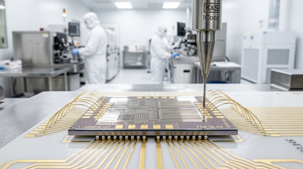

At SEMICON India 2026, the Tata Dholera Fab entered cleanroom fit-out targeting trial wafer production by December 2026, supported by an expanded $13.5 billion India Semiconductor Mission 2.0. Applied Materials committed $5 billion to equipment engineering, while JSR, Sumitomo, and Fujifilm localized critical photoresist chemistry.
For the past three years, international commentary on India’s semiconductor ambitions focused on backend assembly. Setting up Outsourced Semiconductor Assembly and Test (OSAT) and Assembly, Testing, Marking, and Packaging (ATMP) units—such as Micron’s memory packaging plant in Sanand or the CG Semi facility—was a necessary stepping stone. Packaging silicon manufactured abroad creates supply chain muscle, but it does not confer foundry autonomy. The geopolitical risk remains concentrated in the front-end cleanroom: where raw 300mm silicon ingots meet deep ultraviolet (DUV) photolithography scanners, atomic layer deposition chambers, and parts-per-trillion chemical purities.
At SEMICON India 2026, held at the Yashobhoomi Convention Centre in New Delhi, that narrative changed. India’s semiconductor policy transitioned into what the Ministry of Electronics and Information Technology (MeitY) designated as ISM 2.0, backed by an expanded $13.5 billion (approximately ₹1.27 lakh crore) incentive architecture. Instead of subsidizing packaging in isolation, the state and private consortia locked down the four pillars required to sustain commercial wafer production: foundry infrastructure, fab equipment engineering, specialized chemical synthesis, and multi-node capacity commitments.
Front-End Foundry Physics vs. Backend ATMP: The 300mm Chokepoint
To evaluate the engineering transition underway in Gujarat’s Dholera Special Investment Region (DSIR), one must separate backend packaging from front-end fabrication. An ATMP facility receives processed silicon wafers or singulated dies; its operational output is encapsulated, qualified semiconductor packages. The primary tooling consists of wafer dicing saws, die attach pick-and-place units, wire bonders or flip-chip ball grid array (BGA) attachers, transfer molding presses, and automated test handlers.
A front-end 300mm wafer fabrication plant operates under radically different thermodynamic, vibrational, and chemical tolerances. Fabricating an integrated circuit requires cycling a 300mm monocrystalline silicon disk through 500 to 1,200 sequential process steps spanning Deep Ultraviolet (DUV) photolithography, reactive ion etching (RIE), atomic layer deposition (ALD), ion implantation, and chemical-mechanical planarization (CMP).
In this environment, tolerance margins are microscopic. If the purity of electronic-grade anhydrous hydrogen fluoride (99.9999999% or 9N) drops by parts-per-billion, or if the pressure in the ultra-high purity (UHP) chemical loop fluctuates during an active wet strip, active Front Opening Unified Pod (FOUP) lots—each carrying 25 wafers worth hundreds of thousands of dollars—suffer irreversible surface micro-pitting and complete yield collapse. Furthermore, clearing chemical contamination lines and recalibrating mass flow controllers forces days of line starvation, exceeding queue-time limits and corrupting thermal budgets across upstream work-in-progress (WIP) batches.
Water Quality: Standard industrial process water and closed-loop cooling.
Operational Feed: Processed, tested wafers shipped from overseas foundries.
Primary Moat: Die placement accuracy, substrate interconnect density, and testing throughput.
Water Quality: Millions of liters/day of Ultra-Pure Water (18.2 MΩ·cm at 25°C, TOC <1 ppb).
Operational Feed: Blank 300mm monocrystalline p-type silicon wafers.
Primary Moat: ArF immersion lithography overlay, gate dielectric integrity, and defect density yield.
This distinction explains why the construction of the Tata Dholera Fab carries concrete technical weight. The Indian ecosystem is no longer celebrating packaging alone. It is constructing the cleanroom infrastructure, localized chemical pipelines, and tool-maintenance ecosystems required to run an active 300mm wafer line.
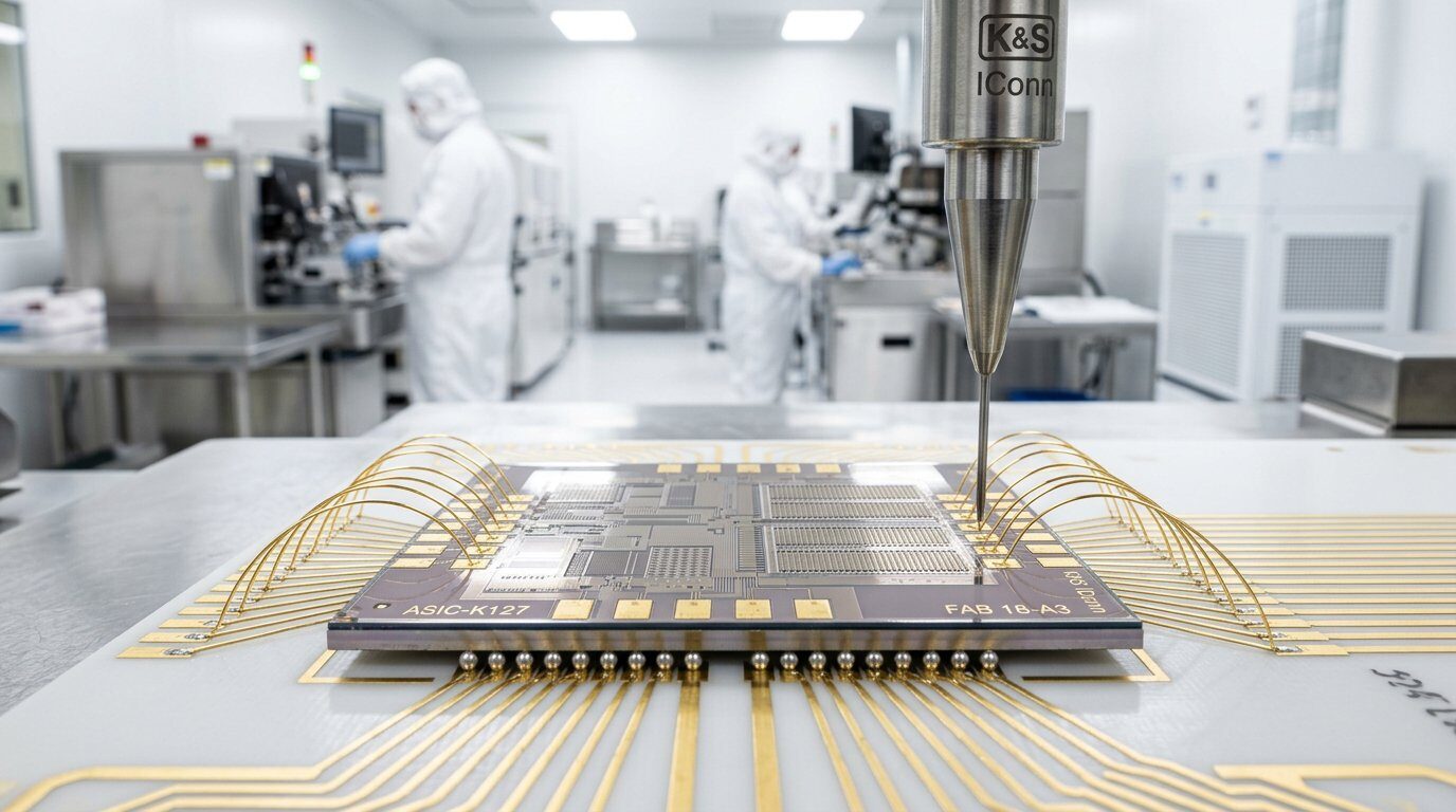
Tata Dholera Fab 1 Architecture: 28nm Planar Nodes, 50,000 WSPM, and PSMC IP Transfer
The Tata Dholera Fab (designated Fab 1) represents an ₹91,000 crore ($11 billion) capital commitment, executed in technical partnership with Taiwan’s Powerchip Semiconductor Manufacturing Corporation (PSMC). PSMC provides mature foundry transfer IP, standard cell libraries, and operating protocols honed across its Hsinchu and Miaoli fabrication sites.
For the Tata Dholera Fab, selecting 28nm, 40nm, 55nm, and 90nm nodes rather than attempting an initial leap to leading-edge sub-5nm FinFET or GAA architectures is rooted in commercial pragmatism. Mature planar CMOS nodes represent over 45% of the total global semiconductor demand by volume. As detailed in our audit of AI inference hardware economics and silicon packaging, every advanced datacenter accelerator or electric vehicle requires dozens of companion microcontrollers, power management ICs (PMICs), and display drivers to operate. Dholera is engineered to capture this high-margin industrial volume.
| Metric / Parameter | Dholera Fab 1 Specification | Strategic Engineering Impact |
|---|---|---|
| Total Capital Outlay | ₹91,000 Crore ($11.0 Billion) | Joint funding via ISM 50% central fiscal incentive + Gujarat state subsidies. |
| Technology Partner | PSMC (Powerchip, Taiwan) | Direct IP transfer for high-voltage CMOS, embedded flash, and logic PDKs. |
| Wafer Size & Full Capacity | 300mm (12-inch) | 50,000 WSPM | Standard commercial 300mm throughput; yield parity targeted across 2 phases. |
| Process Node Allocation | 28nm, 40nm, 55nm, 90nm, 110nm | Avoids EUV scanner capital traps; utilizes mature 193nm ArF immersion DUV lithography. |
| Current Construction Status | 50%+ complete; Cleanroom Fit-Out | Structural framing finished; HVAC air recirculators and vibration slabs active. |
| Production Milestones | Trial Wafers: Dec 2026 | Commercial: 2028 | Commercial capacity pre-allocated across automotive, defense, and power clients. |
The target of December 2026 for trial wafer processing requires that primary tool move-in begins by mid-2026. Installing track systems, wafer steppers, chemical distribution loops, and gas exhausts requires hundreds of certified field application engineers—highlighting the critical role of equipment partnerships announced at the summit.
Applied Materials’ $5 Billion Commitment: Tooling R&D and Local Precision Supply
Semiconductor foundries do not manufacture their own process tools. A commercial fab is an orchestration hub for specialized chambers built by an elite oligopoly: ASML for photolithography scanners, Applied Materials for chemical vapor deposition (CVD), atomic layer deposition (ALD), and chemical-mechanical planarization (CMP), Lam Research for dry plasma etch, and KLA for optical and e-beam defect inspection.
At SEMICON India 2026, Applied Materials announced its “India Vision 2035,” committing $5 billion over the next decade to anchor an advanced engineering and equipment supply ecosystem in the country. The initiative establishes several critical infrastructure layers:
- 140-Acre Advanced Semiconductor Research Park: Establishing a state-of-the-art center in Bengaluru dedicated to semiconductor equipment design, chamber modeling, and sub-assembly validation.
- 10× Local Supply Chain Expansion: Developing Indian precision engineering suppliers capable of manufacturing high-tolerance vacuum valves, gas manifolds, and ceramic components that meet micron-level fab tolerances.
- R&D Workforce Doubling: Expanding Applied Materials’ engineering headcount in India to co-develop next-generation equipment architectures for both domestic lines and global export.
Complementing Applied Materials’ commitment, Lam Research announced an investment of approximately ₹10,000 crore to establish its first silicon component manufacturing facility in India. This plant will support vertical integration from silicon ingot pulling to precision processing of critical consumable parts for plasma etch chambers. When tool chambers require routine maintenance every several thousand wafer passes, having consumable silicon parts and certified service engineers within domestic borders reduces downtime from weeks to hours.
The Electronic Materials Supply Chain: Fujifilm, Sumitomo, and Dholera’s Chemical Hub
While heavy vacuum equipment draws mainstream attention, the operational vulnerability of any semiconductor fab lies in chemical logistics. Silicon manufacturing consumes thousands of metric tons of specialized wet chemicals, ultra-pure gases, and light-sensitive resins. In the 2019 export dispute between Japan and South Korea, restrictions on just three materials—photoresists, hydrogen fluoride, and fluorinated polyimides—threatened to halt South Korean memory production within weeks.
Tata Electronics addressed this vulnerability directly at SEMICON India 2026 through major supply and technical partnerships:
Fujifilm will invest approximately ₹800 crore ($83 million) in phases to establish an advanced semiconductor electronic materials synthesis plant in the Dholera Special Investment Region (DSIR). The facility will formulate high-purity chemical reagents, develop specialized photoresists, and provide technical quality-assurance support to upstream Indian chemical manufacturers.
In parallel, Tata signed strategic agreements with Sumitomo Chemical for semiconductor materials and photoresist supplies, JSR Corporation for lithography chemistry validation, and Kelington Group for ultra-pure piping and bulk gas delivery systems. To house these specialized operations, Tata announced a 363-acre dedicated vendor park adjacent to the Tata Dholera Fab, engineered to accommodate up to 450 certified suppliers. By co-locating chemical purification and wafer fabrication within the same industrial corridor, Dholera insulates its 28nm line from hazardous materials air-freight disruptions.
ISM 2.0 Hardware Matrix: Operational Fabs, Substrates, and OSAT Units Active in 2026
Beyond Dholera, the broader Indian semiconductor ecosystem under ISM 2.0 now includes five operational and development-stage nodes spanning memory, analog packaging, and compound semiconductors:
| Project / Facility | Location | Technology Scope | Operational Status (2026) |
|---|---|---|---|
| Micron ATMP | Sanand, Gujarat | DRAM & NAND Flash Packaging | Commercial production; shipping globally. |
| CG Semi (CG Power + Renesas) | Sanand, Gujarat | Automotive & Industrial OSAT | Active since July 2026; qualified chips delivered. |
| Tata Dholera Fab (Fab 1) | Dholera, Gujarat | 300mm Wafer Fab (28nm–110nm) | Cleanroom fit-out; Dec 2026 trial runs. |
| Tata Electronics OSAT | Jagiroad, Assam | Advanced Flip-Chip & SiP Assembly | Civil construction underway; completion 2027. |
| Kaynes Semicon | Sanand, Gujarat | Power Modules & Micro-controllers | Equipment installation phase. |
This multi-site dispersion balances commercial risk. While Assam handles high-density wire bonding and System-in-Package (SiP) modules for consumer electronics, Gujarat consolidates heavy front-end fabrication and power semiconductor packaging. For systems designers tracking local accelerator deployment, our analysis of silicon architectures and datacenter chips examines how domestic wafer supply will interface with global edge AI platforms.
Technical Due Diligence: 28nm Economics, Tool Move-In, and Yield Calibration
Why did the Tata Dholera Fab prioritize 28nm rather than 3nm?
Sub-5nm fabrication requires extreme ultraviolet (EUV) lithography systems from ASML costing over $350 million per scanner, alongside billions in advanced packaging tooling. In contrast, 28nm planar bulk CMOS is the industry’s sweet spot: it delivers high gate density without moving into complex multi-patterning FinFET economics. Automotive microcontrollers, power management chips, edge AI sensors, and display drivers overwhelmingly rely on 28nm–90nm silicon.
What does Applied Materials’ $5 billion investment actually build?
Applied Materials is not building a commercial wafer foundry. It is investing in a 140-acre semiconductor equipment engineering and research park in Bengaluru. The capital funds precision machining infrastructure, chamber testing laboratories, and domestic supplier onboarding so that Indian component makers can supply vacuum valves, gas delivery lines, and precision hardware to Applied Materials’ global equipment assembly lines.
When will the first commercial chips ship from the Tata Dholera Fab?
Initial trial wafer runs are scheduled to begin by December 2026 to calibrate chamber chemistry and baseline defect density. Full-scale commercial production and customer shipments are scheduled to ramp up progressively, with volume commercial delivery targeted for 2028.