


On a crisp morning in late September 2026, the green marble podium of the United Nations General Assembly in New York echoed with an alarm that sounded less like diplomatic debate and more like an emergency civil defense broadcast. Standing before heads of state, Secretary-General António Guterres drew an explicit, unsettling parallel between Cold War nuclear brinkmanship and the server racks powering modern artificial intelligence. His message was unambiguous: frontier compute was accelerating beyond humanity’s ability to govern it, hurtling toward an existential threshold that demanded immediate, binding global treaties and planetary-scale emergency brakes.
Yet, at that exact hour, across eight time zones, a completely different set of documents was being initialed in near-total silence.
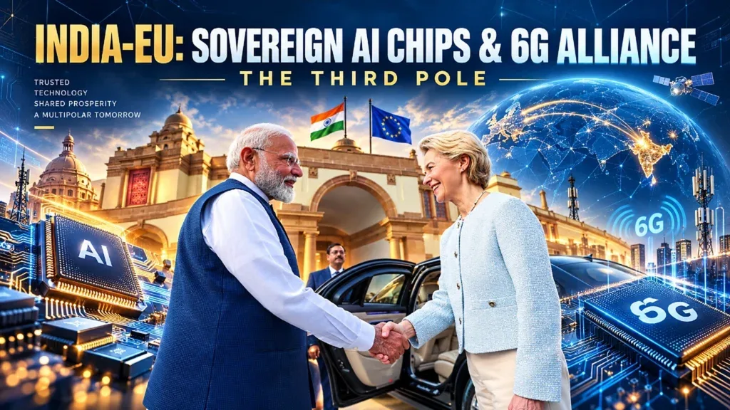
Inside the secure negotiating rooms of the India-EU Trade and Technology Council (TTC) spanning Brussels and New Delhi, nobody was drafting a moratorium. Nobody was preparing a shutdown treaty. Instead, senior industrial envoys and systems architects were finalizing the confidential technical annexes for an audacious counter-offensive: the India-EU AI chip and 6G alliance—a coordinated, bilateral mobilization to manufacture custom artificial intelligence silicon, establish independent semiconductor supply chains, and build out the world’s first integrated sub-terahertz 6G telecommunications corridors.
Why would two of the world’s largest democratic blocs—representing two billion citizens and a combined economic output exceeding $23 trillion—choose this precise moment to break ranks with the United Nations’ existential consensus?
The answer lies far beneath the diplomatic rhetoric, buried inside the unforgiving physics and economics of modern computing. To strategic planners in New Delhi and Brussels, the genuine existential threat is not a distant, speculative superintelligence escaping a research lab. The existential threat is digital vassalage—the realization that the critical infrastructure of both economies, from power grids and autonomous defense systems to financial ledgers, is currently captive to two foreign monopolies: the proprietary cloud empires of the United States and the state-subsidized compute engine of China.
If a sovereign nation does not own the physical instruction sets etched into its silicon, its sovereignty exists only on paper.
What India and the European Union are assembling is not another diplomatic communiqué. It is a hardened Third Technopolitical Pole. By fusing Europe’s near-monopoly on extreme ultraviolet research pilot lines at imec with India’s 20% share of global chip design talent and the massive semiconductor foundries rising in Gujarat, the alliance is executing an end-to-end bypass of American and Chinese gatekeepers.
And deep inside their shared architectural blueprints sits an obscure, non-negotiable physical constraint: 27.2 microseconds. In that razor-thin slice of time, the entire battle over who controls the future of artificial intelligence is quietly being fought.
The India-EU AI Chip and 6G Alliance: Architecture of the Third Pole
The geopolitical realignment underway between Brussels and New Delhi is grounded in cold industrial realpolitik. For decades, global digital power was defined by software applications and service contracts. In 2026, power is defined by the physical substrate: lithography tools, atomic-scale gate designs, sub-terahertz spectrum allocations, and firm power delivery.
The India-EU AI chip and 6G alliance is an intergovernmental industrial framework executing under the India-EU Trade and Technology Council (TTC). It integrates the India Semiconductor Mission (ISM Phase 2) with the European Chips Act (€47B), establishing a bi-regional silicon design corridor, shared RISC-V compute engines, Universal Chiplet Interconnect Express (UCIe) packaging standards, and harmonized sub-terahertz (100–300 GHz) spectrum between the Bharat 6G Alliance and the EU 6G-IA.
To understand the scale of this sovereign counter-weight, consider the stark structural divergence across the three dominant technopolitical blocs:
| Architectural Layer | United States (Hyperscale Monolith) | China (State-Subsidized Abundance) | India-EU Alliance (Third Pole) |
|---|---|---|---|
| Core Compute ISA | Proprietary x86 & ARMv9; NVIDIA CUDA hardware locks | Huawei DaVinci / Ascend CANN; LoongArch; proprietary forks | Open RISC-V (DIR-V Shakti/Vega + EPI SiPearl Rhea) |
| Fab & Packaging | TSMC Arizona / Oregon; Intel IFS; CoWoS-L packaging bottlenecks | SMIC DUV multi-patterning (SAQP); domestic HiZQ HBM clusters | imec 2nm pilot lines + Tata Dholera / Kaynes OSAT + STMicro |
| Telecom Interconnect | 5G Standalone; carrier cloud integration (AWS Wavelength/Azure) | Massive 5G-Advanced footprint; Huawei single-vendor vertical stack | Bharat 6G + 6G-IA joint sub-THz ISAC (130–330 GHz) |
| Interconnect Standard | NVLink 5 (proprietary); Ultra Ethernet Consortium (UEC) | UnifiedBus / HCCS proprietary scale-up fabric | Universal Chiplet Interconnect Express (UCIe) + CPO |
| Existential AI Stance | Voluntary commitments; frontier model licensing; defense integration | CAC algorithmic registries; socialist core value alignment | Sovereign industrial defense; statutory safety via EU AI Act + India DPDP |
Connecting Tata Dholera and imec Pilot Lines: The Silicon Pipeline
The physical foundation of the India-EU technopolitical bloc is built on a concrete mutual dependency: Europe possesses the world’s most advanced semiconductor R&D tooling but lacks packaging scale and a domestic consumer electronics volume sink; India possesses massive design talent and assembly capacity but lacks advanced lithography infrastructure.
Under the European Chips Act, the EU committed €47 billion to bolster continental semiconductor manufacturing, highlighted by the establishment of advanced pilot lines at imec in Leuven, Belgium, CEA-Leti in Grenoble, France, and the Fraunhofer Institute in Germany. As analyzed in our teardown of TSMC’s 2nm GAAFET transition, leading-edge pilot facilities lead the world in post-FinFET scaling: exploring 2nm Gate-All-Around (GAAFET) architectures, Complementary FETs (CFET), and backside power delivery networks (BSPDN).
However, Europe’s commercial fabs—dominated by STMicroelectronics, NXP, and Infineon—are primarily optimized for 28nm to 90nm trailing nodes tailored for automotive microcontrollers, power discretes, and industrial sensor silicon. Europe does not operate a commercial high-volume leading-edge logic fab.
Simultaneously, India’s Semiconductor Mission (ISM), backed by an initial $10 billion incentive outlay and preparing for an expanded Semicon 2.0 capitalization round, has aggressively broken ground on commercial facilities, reflecting the massive industrial expansion detailed in our audit of Goldman Sachs’ 42 Indian AI infrastructure enablers:
- Tata Electronics’ Fab in Dholera, Gujarat: A $11 billion partnership with Taiwan’s Powerchip Semiconductor Manufacturing Corporation (PSMC), targeting 28nm, 40nm, and 91nm planar and FinFET production with an eventual capacity of 50,000 wafer starts per month.
- Advanced OSAT / ATMP Facilities: Tata’s packaging facility in Jagiroad, Assam ($3.2B), the CG Semi facility in Sanand ($900M), and the Kaynes Semicon unit in Gujarat, focusing on advanced multi-chip packaging, ball grid arrays, and optical transceivers.
The operational synthesis works through a modular 2.5D/3D Chiplet Architecture. Rather than attempting to match TSMC’s monolithic 2nm wafer yields—a multi-billion-dollar capital expenditure that neither Europe nor India can justify alone—the alliance leverages the open Universal Chiplet Interconnect Express (UCIe 2.0) standard. Leading-edge European pilot lines fabricate specialized, low-area neural accelerator tiles (NPUs) on sub-3nm GAAFET nodes, which are then integrated over silicon interposers with 28nm I/O, power management, and memory control dies manufactured and packaged at Tata’s Dholera and Sanand complexes.
This modular strategy eliminates the single-foundry chokepoint. If high-density compute logic is fabricated in Europe or licensed through trusted partners, while baseband processing, power electronics, and final heterogeneous assembly are executed in India, both entities retain sovereign control over the critical bill of materials without depending on Taiwanese packaging foundries that sit within range of regional geopolitical tensions.
Instruction Set Independence: RISC-V Bypasses x86 and ARM Chokepoints
To build sovereign AI accelerators, physical lithography is only half the battle; the instruction set architecture (ISA) is the software gatekeeper.
Historically, global compute has been trapped within a duopoly of proprietary instruction sets:
- x86: Controlled exclusively by Intel and AMD through a complex web of cross-licensing patents that prevent any new market entrant from designing compatible high-performance server silicon.
- ARM: Owned by SoftBank, which has aggressively restructured its licensing models, escalated IP litigation against licensees, and increased royalty fees while enforcing restrictive core implementation rules.
For India and the European Union, licensing proprietary ISAs introduces unacceptable geopolitical vulnerabilities. The United States can, by executive decree via the Bureau of Industry and Security (BIS), weaponize export control regimes to revoke architecture access or restrict compute performance thresholds overnight, a risk mirrored in China’s state-backed migration examined in our breakdown of DeepSeek’s reliance on Huawei Ascend 950DT silicon.
The answer is RISC-V—an open-standard, royalty-free instruction set governed by RISC-V International, headquartered in Switzerland precisely to remain neutral from extraterritorial trade restrictions.
Both regions have spent years developing independent RISC-V competencies:
- India’s Digital India RISC-V (DIR-V) Program: Spearheaded by the Ministry of Electronics and Information Technology (MeitY), DIR-V has funded domestic processor cores including Shakti (developed by IIT Madras) and Vega (developed by C-DAC). More critically, C-DAC’s high-performance computing roadmap has yielded the AUM processor—a dual-socket, 96-core enterprise chip designed for supercomputing clusters.
- Europe’s European Processor Initiative (EPI): A consortium of 30 partners across 10 European countries tasked with building sovereign supercomputing and automotive chips. The project’s commercial vehicle, SiPearl, has designed the Rhea series of high-memory-bandwidth processors, collaborating with French chipmaker Cortus and Spain’s Barcelona Supercomputing Center (BSC) to engineer custom RISC-V vector accelerators.
Under the expanded TTC semiconductor track, India and the EU are synchronizing their RISC-V compiler stacks and hardware acceleration extensions. Instead of each entity maintaining fragmented, custom instruction extensions for tensor math, the joint working groups are standardizing the RV-AI matrix acceleration pipeline.
Hardware Bottleneck Analysis: Because off-chip memory access consumes nearly two orders of magnitude more energy than on-chip arithmetic (approximately 20 pJ/bit vs. 0.2 pJ/bit), the joint RISC-V specification bypasses Von Neumann memory bottlenecks, avoiding the steep developer compute ceilings analyzed in our guide to production AI hardware requirements. It couples tightly integrated SRAM scratchpads with systolic 16-bit brain-floating-point (BF16) and 8-bit microscopic scaling units (FP8) directly to the RISC-V vector register file, dramatically optimizing the Energy-Delay Product (EDP) for edge inference.
By standardizing this interface at the hardware description level (RTL), Indian design startups (like Mindgrove Technologies and InCore Semiconductors) and European industrial silicon suppliers can drop verified, open-source neural processing units into custom ASICs without paying recurring licensing fees to foreign proprietary IP vendors.
6G Compute-Network Convergence: Sub-THz Telecommunications at 140 GHz
The second pillar of the partnership bridges compute silicon directly into the cellular transport medium.
In public discourse, telecommunications generations are often viewed merely as consumer bandwidth upgrades: 4G enabled mobile video streaming; 5G enabled high-density device connectivity and lower latency.
6G is fundamentally different: it is an edge-compute distribution architecture.
Compute-Network Convergence (CNC) in 6G represents the complete structural unification of telecommunications transport and distributed artificial intelligence computing. Under CNC, base stations cease to be passive transceivers; they function as distributed inference execution nodes running on-device microVMs and eBPF routing to process autonomous agent tasks within sub-millisecond latencies, formally standardized in ITU-R Recommendation M.2160 (IMT-2030).
In June 2024, the Bharat 6G Alliance and the European 6G Smart Networks and Services Industry Association formalized their bilateral alignment, submitting harmonized technical work items to the International Telecommunication Union (ITU-R IMT-2030) and the 3rd Generation Partnership Project (3GPP Releases 20 and 21).
Why does this require a joint chip alliance?
Because operating at sub-terahertz frequencies presents brutal physical and thermodynamic constraints. At 140 GHz, atmospheric attenuation, molecular oxygen absorption, and extreme path loss demand massive antenna arrays (Massive MIMO with 1,024+ elements) executing real-time digital beamforming.
Calculating phase shifts and dynamic beam tracking for hundreds of high-speed mobile nodes in microsecond intervals cannot be routed back to a centralized cloud. It requires dedicated, low-power neural beamforming ASICs integrated directly at the Distributed Antenna Unit (DAU). The custom RISC-V chips being developed under the TTC are the exact silicon engines designed to be mounted onto European (Ericsson, Nokia) and Indian (Tejas Networks, C-DOT) radio heads.
Thermodynamic and Path-Loss Constraints at 140 GHz
Operating communication systems in the sub-terahertz regime requires overcoming severe non-linear physical phenomena that do not exist in conventional sub-6 GHz or standard millimeter-wave deployments.
Physical Attenuation Mechanics: Beyond classical geometric spreading loss, sub-THz electromagnetic signals suffer severe atmospheric attenuation caused by the resonance absorption lines of water vapor (H2O) and molecular oxygen (O2), which spike aggressively around 183 GHz and 325 GHz. Maintaining a viable communication link across an urban 200-meter micro-cell radius requires massive directional antenna gain exceeding 40 dBi, demanding the deployment of ultra-dense silicon beamforming arrays capable of sub-millidegree phase tracking.
This physical barrier dictates an unforgiving temporal boundary: the 27.2 microsecond Doppler coherence window. At 140 GHz with a mobile receiver in transit at 120 km/h, the channel coherence time drops to approximately 27.2 microseconds. Any beamforming neural model that takes longer than 27 microseconds to infer and adjust antenna phase weights loses the link completely. This proves why cloud-hosted inference cannot operate a 6G sub-terahertz network: the physical propagation delay of routing light through a fiber link to a centralized data center and back (roughly 1 millisecond per 100 kilometers) is forty times longer than the physical survival window of the radio link itself.
Because the atmospheric path loss is so severe, 6G cells will feature small physical radii (between 50 and 200 meters). In an urban center like Mumbai, Paris, Berlin, or Bengaluru, millions of these micro-cells will blanket the landscape.
If every micro-cell required an expensive, high-power American GPU to manage its real-time neural beamforming, the telecommunications grid would collapse under immense capital and energy costs, a dynamic exposed in our forensic audit of cloud GPU pricing and egress taxes. The India-EU partnership directly answers this constraint: custom, ultra-low-power RISC-V edge silicon fabricated via cost-effective modular packaging that consumes less than 5 Watts per antenna unit.
The Geopolitical Moat: Sovereign Compute vs. Cloud Vassalage
The structural divergence between the UN’s existential warnings and the India-EU industrial alliance reveals an undeniable geopolitical reality: the era of unified global technology governance has ended.
The United Nations operates under the assumption that technology can be governed via multilateral consensus, harmonized treaties, and international verification regimes. But this model assumes that all participating nation-states share identical economic conditions, threats, and sovereign objectives.
In reality, the global digital economy is separating into rival technological ecosystems, contrasting the proprietary hyperscale clouds of the United States and state-subsidized hardware of China with the emerging sovereign open-compute “Third Pole” of the India-EU corridor.
Why can neither India nor Europe accept the UN’s call for centralized compute restrictions?
1. The European Vulnerability: Regulation Without Industrial Capacity
For the past decade, the European Union pursued technology policy through the “Brussels Effect”—the belief that by enacting gold-standard regulations (such as GDPR, the Digital Markets Act, and the EU AI Act), it could force multinational tech monopolies to conform to European norms.
However, European leaders realized this approach had created a fatal structural weakness: Europe regulated the digital economy, but American corporations owned it.
European banks, healthcare systems, defense ministries, and automakers run their mission-critical workloads on Amazon Web Services, Microsoft Azure, and Google Cloud, powered almost exclusively by NVIDIA silicon. If the United States were to impose export restrictions or if cross-border data transfer agreements broke down, Europe’s domestic economy would face immediate operational paralysis. For the EU, co-developing sovereign silicon with India is an urgent prerequisite for true strategic autonomy.
2. The Indian Vulnerability: Demographic Scale Trapped in Foreign APIs
India faces the reciprocal side of the same structural dilemma. With 1.4 billion citizens, over 950 million broadband subscribers, and the world’s highest average monthly data consumption (exceeding 31 GB per user per month), India is the largest consumer market for digital services on earth. Furthermore, India’s software engineering workforce (over 5.4 million developers) and global capability centers (GCCs) design approximately 20% of the world’s cutting-edge semiconductor chips for foreign multinational corporations.
Yet, despite this massive talent pool, India does not own the intellectual property or the physical fabrication plants that manufacture these chips. If India were to comply with global moratoriums that restrict compute expansion, it would permanently lock its demographic dividend into a low-margin IT services role—renting AI tokens from American foundational model providers at retail rates while writing software for foreign hardware platforms.
By building a sovereign hardware and telecommunications corridor with Europe, India transitions from being an outsourced service provider into a primary owner of global compute architecture.
The Engineering Blueprint: A 4-Tier Interoperability Stack
To execute this vision, the joint India-EU working group has outlined an integrated, open-source reference architecture. Rather than building a closed vertical silo, the architecture establishes four vendor-neutral layers connecting Indian chip design and European pilot foundries, enabling the deployment of autonomous systems such as those explored in our analysis of managed agent execution harnesses:
What is the India-EU AI chip and 6G alliance?
The India-EU AI chip and 6G alliance is an institutionalized technology corridor established under the Trade and Technology Council (TTC). It couples the European Chips Act pilot lines (imec, CEA-Leti) and automotive silicon leaders with the India Semiconductor Mission (ISM) packaging hubs (Tata Dholera, Kaynes, CG Semi), while standardizing open RISC-V accelerators and sub-terahertz (100–300 GHz) 6G spectrum between the Bharat 6G Alliance and EU 6G-IA.
Why does the alliance break ranks with the UN position on existential AI risk?
While UN Secretary-General António Guterres at UNGA 81 advocated for nuclear-style non-proliferation treaties and compute moratoriums, India and the EU determined that unilateral deceleration leads directly to digital vassalage. Halting domestic infrastructure would lock both economies into permanent reliance on American hyperscaler monopolies or Chinese state-subsidized compute.
Why is on-device neural acceleration required for 6G sub-terahertz beamforming?
At 140 GHz, high mobility causes the physical Doppler coherence time of the wireless channel to collapse to just 27.2 microseconds. Routing telemetry back to centralized cloud data centers takes milliseconds—far too slow to prevent beam dropouts. Dedicated on-chip RISC-V neural accelerators mounted at Distributed Antenna Units (DAU) are physically required to calculate beam trajectories in real time.
Access the EyesTech Sub-THz Link Budget, Atmospheric Path-Loss Modeling, and Coherence Time Simulation Suite for 6G Compute-Network Convergence.