
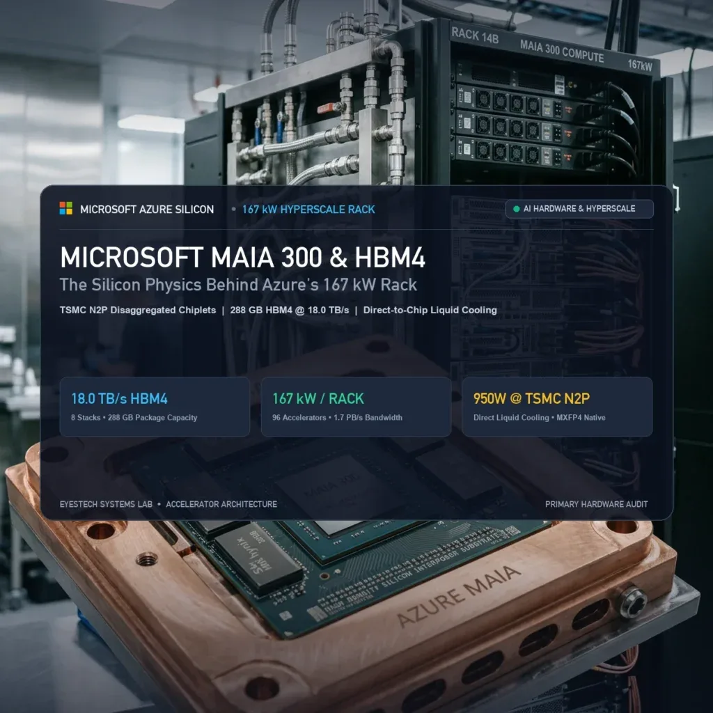

Microsoft’s Maia 300 accelerator integrates 288 GB of HBM4 memory delivering 18.0 TB/s of peak bandwidth across eight 3D-stacked dies fabricated on TSMC’s N2P node. Operating at a 950W thermal design power, 96 Maia 300 accelerators are clustered within a single 167-kilowatt direct-to-chip liquid-cooled rack delivering 27.6 TB of high-bandwidth memory and 1.7 PB/s of aggregate throughput for multi-gigawatt production Azure rollouts scheduled for 2027.
The mainstream technical press has framed the announcement through the familiar corporate narrative of cloud hyperscalers escaping Nvidia’s 75% gross margins. But when you strip away financial commentary and examine the bare die packaging, the Maia 300 is not merely a cost-hedging merchant silicon replacement. It is a radical architectural departure designed to address a brutal physical reality: frontier transformer inference is choked by memory bandwidth and thermal dissipation, not raw matrix multiply operations.
In our newsroom’s October 10 analysis of OpenAI’s 10 GW ASIC alliance with Broadcom and TSMC, our colleague Lukas Schmidt documented how contractual absorption commitments would force Microsoft Azure to prioritize datacenter floor space and thermal envelopes for custom silicon. The physical manifestation of that prioritization has now arrived. By packing 96 accelerators into a 167 kW thermal envelope, Microsoft is redefining the volumetric density of AI compute—at the expense of requiring complete facility-level cooling overhauls that standard 40 kW hyperscale halls cannot support.
The Memory Wall: Why Azure Bet on 18.0 TB/s HBM4
In modern autoregressive decoding, every generated token requires streaming every parameter of a multi-billion-parameter model from off-chip memory into execution registers. As I documented in our teardown of FeSens openTPU and agent-synthesized RTL, even specialized matrix engines suffer catastrophic throughput collapse—dropping from dozens of tokens per second down to single digits—the instant model weights outstrip local cache and encounter physical memory bandwidth limits.
To overcome this bottleneck, the Maia 300 shifts from the 1024-bit physical interface of HBM3e to JEDEC’s next-generation HBM4 standard. Under HBM4, each memory stack features a 2048-bit wide interface—doubling the pin count per stack. By mounting eight HBM4 stacks around its disaggregated compute complex, Maia 300 commands a 16,384-bit wide memory bus, streaming data at an unprecedented 18.0 TB/s. This represents a 2.25× bandwidth expansion over Nvidia’s GB200 NVL72 (which routes 8.0 TB/s of HBM3e per Blackwell package).
Hardware Bottleneck Analysis: In single-stream or low-batch inference, arithmetic intensity collapses to I ≈ 1 FLOP/byte. For a 70B parameter model in 4-bit precision (35 GB weight footprint), Maia 300’s 18.0 TB/s bandwidth reduces memory read latency to Tread = 35 GB / 18,000 GB/s = 1.94 milliseconds per token (514 tokens/sec theoretical ceiling), compared to 4.38 ms on 8.0 TB/s HBM3e baselines.
Beyond raw HBM4 bandwidth, Microsoft engineers incorporated an on-chip, software-defined SRAM scratchpad cache. By staging attention Key-Value (KV) cache heads and active weight tiles directly in high-density SRAM adjacent to the systolic tensor units, the chip bypasses the HBM physical layer entirely for intermediate activations. This hybrid memory hierarchy drastically reduces read amplification and mitigates memory bus contention during concurrent multi-tenant serving.
Silicon Disaggregation on TSMC N2P: The Chiplet Latency Tax
To fabricate an accelerator capable of orchestrating 288 GB of HBM4, Microsoft could not rely on a monolithic silicon die. With TSMC’s EUV lithography reticle limit capped at approximately 858 mm², attempting to print compute arrays, dual-channel HBM4 memory PHYs, and massive scale-out optical interconnects on a single piece of silicon results in dismal wafer yields and catastrophic unit costs.
Instead, Microsoft adopted a disaggregated multi-die chiplet architecture manufactured on TSMC’s leading-edge N2P process node. TSMC N2P introduces backside power delivery networks (BSPDN)—which TSMC terms SuperPowerRail—separating the power distribution grid from signal routing layers on the front of the wafer. This architecture eliminates IR voltage drops across dense compute cores, enabling higher clock frequencies at lower operational voltages.
However, disaggregation introduces a fundamental physical trade-off: cross-chiplet interconnect latency. While compute dies sit on N2P, the memory controllers and high-speed SerDes I/O tiles are split onto separate silicon dies interconnected via high-density packaging. Even with sub-micron micro-bumps and silicon interposers, traversing die-to-die (D2D) boundaries adds an unavoidable 12 to 18 nanoseconds of round-trip latency. If the compiler scheduler fails to overlap compute passes with memory staging, the execution pipeline stalls—nullifying the raw bandwidth benefits of HBM4.
Constrained by the 858 mm² reticle boundary. Yield drops exponentially with die area. Forced compromises between on-die SRAM capacity and tensor core count.
Decouples N2P compute engines from I/O and HBM4 controllers. Yields improve dramatically, but exposes a 12–18 ns cross-chiplet bus latency penalty that demands software-managed SRAM caching.
Microscaling MXFP4: Compressing Weights Without Per-Token Precision Collapse
To maximize compute density within each 950W accelerator, Maia 300 introduces dedicated execution pipelines for the Open Compute Project (OCP) Microscaling MXFP4 specification. Unlike standard uniform FP4 quantization, which quantizes an entire tensor or row with a single scaling factor, Microscaling groups small vectors of 32 values (block size k = 32) and assigns them a shared 8-bit scale factor (E8M0).
This fine-grained blocking maintains numerical stability during matrix multiplications, eliminating the outlier activation spikes that typically degrade perplexity in sub-8-bit models. Native MXFP4 silicon delivers 13.8 PFLOPS of peak inference compute per Maia 300 chip. Crucially, executing operations in 4-bit representation halves the memory footprint of transformer weights, effectively doubling the capacity of the 288 GB HBM4 package and allowing 400B+ parameter models to reside within a compact accelerator footprint without cross-node network sharding.
The 167 kW Rack: Direct-to-Chip Liquid Cooling Physics
The most consequential engineering metric of the Maia 300 program is not its silicon area or its FLOPS rating. It is the rack power density: 167 kilowatts.
In standard enterprise and legacy cloud datacenters, server racks operate between 15 kW and 40 kW. At 40 kW, high-velocity chilled air moving across massive finned heatsinks can still maintain silicon junction temperatures below the 85°C throttling threshold. At 167 kW per rack—housing 96 Maia 300 accelerators across 24 four-node trays—air cooling becomes physically impossible. Air simply lacks the volumetric heat capacity to extract 167 kilojoules of thermal energy per second without hurricane-force fan walls that consume prohibitive auxiliary power, as we detailed in our examination of Nvidia’s air-cooled fan-tax compromises.
Heat Rejection Calculation: For a 167 kW thermal load (Q̇ = 167,000 W) using treated water coolant (Cp ≈ 4,184 J/(kg·K)) across an allowable temperature delta ΔT = 10 K (32°C supply to 42°C return):
ṁ = 167,000 / (4,184 · 10) = 3.99 kg/s ≈ 240 Liters per minute (63.4 GPM).
Circulating 240 L/min through microchannel cold plates across 96 dies demands custom Coolant Distribution Units (CDUs) operating at 35–45 psi, with zero-drip blind-mate hydraulic manifolds.
Each Maia 300 chassis mates directly to an in-rack stainless-steel liquid manifold via blind-mate quick-disconnect couplings. Chilled coolant circulates directly through microchannel cold plates clamped to the TSMC N2P silicon and the eight flanking HBM4 stacks, removing over 95% of heat directly to water loops before secondary rear-door heat exchangers dissipate the residual baseline.
Architectural Teardown: Maia 300 vs. Industry Baselines
To understand where Microsoft’s custom hardware stands against merchant alternatives from Nvidia and AMD, we examine the primary silicon and rack telemetry across compute, memory, and thermal dimensions:
| Architectural Dimension | Microsoft Maia 300 | Microsoft Maia 200 | Nvidia GB200 NVL72 | AMD Instinct MI350X |
|---|---|---|---|---|
| Process Node | TSMC N2P (Disaggregated) | TSMC N3E | TSMC 4NP (CoWoS-L) | TSMC N3P / N4 |
| Memory Technology | 8× HBM4 (2048-bit PHY) | 4× HBM3e | 8× HBM3e (1024-bit PHY) | 8× HBM3e |
| HBM Capacity per Package | 288 GB | 96 GB | 192 GB (per Blackwell) | 288 GB |
| Peak Memory Bandwidth | 18.0 TB/s | 4.8 TB/s | 8.0 TB/s | 8.0 TB/s |
| TDP per Accelerator | 950 Watts | 600 Watts | 1,200 Watts | 1,000 Watts |
| Accelerators per Rack | 96 | 48 | 72 | 64 (Standard 8-way OAM) |
| Aggregate Rack Memory | 27.6 TB | 4.6 TB | 13.8 TB | 18.4 TB |
| Aggregate Rack Bandwidth | 1.728 PB/s | 0.230 PB/s | 0.576 PB/s | 0.512 PB/s |
| Total Rack Thermal Envelope | 167 kW | 42 kW | 120–132 kW | 80–90 kW |
| Cooling Architecture | Direct-to-Chip Liquid (240 L/min) | Hybrid Air / Cold Plate | Direct-to-Chip Liquid | Facility Water / RDHx |
The Datacenter Deployment Divide: 2027 Multi-Gigawatt Realities
Microsoft asserts that Maia 300 delivers 40% higher token throughput per megawatt compared to contemporary GPU clusters, yielding a 7× rack-scale throughput multiplier over the previous Maia 200 generation. However, hyperscale silicon efficiency claims must be evaluated alongside facility-level economics, an operational tension my colleague Prithu Vardhan Mishra explored in our investigation of Qualcomm and AWS’s $60 billion silicon pact.
While Maia 300 dramatically compresses whitespace footprint by condensing 1.7 PB/s of bandwidth into a single floor tile, it cannot be dropped into standard Azure datacenter capacity. Deploying a 167 kW rack topology requires dedicated high-density datacenter halls equipped with isolated medium-voltage power distribution, dual 415V three-phase busways, and subterranean hydraulic plumbing loops capable of continuous multi-thousand gallon per minute heat rejection.
For Microsoft, the 2027 multi-gigawatt production timeline reflects this facility buildout bottleneck rather than silicon fabrication delays at TSMC. The silicon physics of the Maia 300—pairing N2P disaggregated chiplets with 18.0 TB/s HBM4—solve the algorithmic memory wall. Whether Azure can provision gigawatts of 167 kW liquid-cooled whitespace rapidly enough to capture the economic upside remains the decisive engineering challenge.
Frequently Asked Questions: Microsoft Maia 300 Architecture
What differentiates Microsoft Maia 300 from Nvidia’s Blackwell GB200?
While Nvidia GB200 uses 8.0 TB/s HBM3e on a 1024-bit bus, Maia 300 integrates JEDEC HBM4 across a 2048-bit interface per stack, achieving 18.0 TB/s per accelerator—a 2.25× memory bandwidth advantage. Maia 300 also features on-chip software-defined SRAM scratchpads to bypass HBM for active KV cache heads.
Why does Maia 300 operate within a 167 kW rack power envelope?
Packing 96 accelerators (each with a 950W TDP) alongside host CPUs, PCIe switching, optical transceivers, and voltage regulators totals 167 kW. This high volumetric density maximizes token throughput per square foot of datacenter whitespace, but mandates dedicated direct-to-chip liquid cooling capable of circulating 240 liters of coolant per minute.
What precision format does Maia 300 use for low-latency inference?
Maia 300 features native execution units for the OCP Microscaling MXFP4 specification. By scaling small 32-element vectors with a shared 8-bit scale factor, it maintains numerical stability while doubling compute throughput and halving memory consumption compared to FP8.