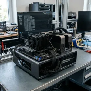


FeSens openTPU demonstrates that autonomous AI agents can generate synthesizable, timing-closed hardware description language for neural acceleration, achieving 85.8 tokens per second decoding LFM2.5-230M on a Xilinx Kintex-7 xc7k480t FPGA. However, multi-billion parameter architectures like Gemma 4 and Qwen3.5 collapse to 1–4 tokens per second because agent-synthesized RTL cannot circumvent physical off-chip memory bandwidth constraints.
The Closed-Loop Tournament Behind OpenTPU
The foundational ambition of recursive self-improvement in computer engineering has long centered on a closed loop: machine learning models optimizing the silicon floorplans that execute their own inference passes. The open-source FeSens openTPU repository converts that theoretical objective into a working hardware artifact. Developed as an extension of the auto-arch-tournament framework—which previously deployed competitive language model agents to iterate RISC-V CPU pipelines—openTPU utilizes Claude Opus 5.5 to author, refactor, and verify synthesizable SystemVerilog modules inside an automated hardware regression harness.
Rather than producing disconnected Verilog snippets, the openTPU monorepo maintains four tightly coupled layers:
- Synthesizable SystemVerilog RTL: A modular execution engine comprising a top-level sequencer, Direct Memory Access (DMA) channels, a systolic matrix multiplication unit, a vector arithmetic unit, and an activation quantizer.
- Custom Tensor ISA: A dedicated instruction set architecture engineered specifically for quantized matrix-vector contractions, bypassing the instruction fetch and decode overhead of general-purpose RISC architectures.
- Bit-Exact Python Reference Simulator: A software golden model that executes identical tensor operations at cycle boundaries, acting as the mathematical verification oracle against which all RTL modifications are tested.
- Python Kernel Compiler & Profiler: A toolchain that compiles model computation graphs into scheduled openTPU micro-operations, generating cycle-accurate hardware profiling traces.
During each tournament iteration, Claude Opus 5.5 proposes architectural modifications—such as tuning pipeline register stages or restructuring ping-pong memory banking—to maximize clock frequency and reduce operational stall cycles. The proposed SystemVerilog is compiled against the bit-exact Python simulator. Any proposed diff that introduces functional deviation, fails formal regression tests, or violates timing closure in the AMD Vivado synthesis flow is discarded, with the synthesis log errors automatically recycled into the agent prompt context.
Architectural Friction: Why OpenTPU Discards Caches
In commercial GPU and accelerator architectures, substantial die real estate is dedicated to multi-level cache hierarchies, out-of-order execution windows, and dynamic branch prediction logic. When language models attempt to design hardware, these deeply coupled state machines frequently fail verification due to race conditions and edge cases in cache coherency protocols.
FeSens solved this friction through deliberate architectural subtraction: openTPU contains zero hardware-managed caches and zero speculative execution logic.
Instead of relying on hardware cache arbitration, the core utilizes software-managed on-chip scratchpad SRAM tiles arranged in double-buffered ping-pong configurations. While the systolic matrix unit computes forward contractions using weights buffered in Bank A, autonomous DMA engines stream subsequent parameter tiles from host DRAM across PCIe into Bank B. This deterministic pipeline guarantees that the kernel compiler knows the exact clock cycle each matrix element reaches the arithmetic register file.
The synthesized architecture was flashed onto an Inspur YPCB-00338 PCIe add-in card hosting an AMD/Xilinx Kintex-7 xc7k480t FPGA. This silicon target provides 477,760 logic cells, 1,920 DSP48E1 arithmetic slices, 34,380 Kb of dual-port Block RAM (~4.2 MB), and 2,870 KB of distributed LUT-RAM, communicating with host memory over a PCIe Gen3 interconnect.
Empirical Telemetry: Throughput Across Model Classes
Hardware traces recorded on the physical Inspur YPCB-00338 FPGA board reveal extreme performance bifurcation between models that fit within local on-chip buffers and architectures that must stream weights from off-chip memory:
| Model Architecture | Active Parameters | Quantization | Decode Speed | Prefill Speed | Primary Execution Constraint |
|---|---|---|---|---|---|
| LFM2.5 (Liquid) | 230M | INT4 Custom | 85.8 tok/s | 335.4 tok/s | DSP Pipeline Latency (In-SRAM) |
| LFM2.5 (Liquid) | 230M | INT8 Precision | 59.0 tok/s | 295.6 tok/s | BRAM Bank Width Capacity |
| Qwen3.5-35B-A3B | 3.2B Active (MoE) | INT4 Quantized | 3.95 tok/s | 14.2 tok/s | PCIe Expert Parameter Streaming |
| Phi-4-mini | 3.8B Dense | INT4 Quantized | 3.80 tok/s | 11.8 tok/s | Off-Chip DDR3 Memory Bandwidth |
| Gemma 4 | 2.6B Dense | INT4 Quantized | 4.10 tok/s | 16.5 tok/s | Memory Controller Burst Saturation |
| Qwen3.5 | 4.0B Dense | INT4 Quantized | 2.10 tok/s | 9.4 tok/s | External Memory Bus Stalls |
When evaluating sub-billion parameter models like LFM2.5-230M, weights fit entirely into the Kintex-7’s high-speed distributed SRAM, allowing the DSP array to execute without external DRAM wait states. At 85.8 tokens per second in 4-bit mode (and 82.1 tok/s inclusive of Python runtime host overhead), the agent-designed RTL performs on par with commercial edge NPUs.
However, as soon as a model exceeds on-chip memory capacity, token generation throughput plunges by over 95%. When we documented the physical packaging limits of custom AI ASICs, we highlighted that peak arithmetic FLOPS become unusable without proportional interconnect scaling. openTPU provides a stark, physical validation of this dynamic on edge hardware.
The Arithmetic Reveal: Calculating the Memory Wall
The 20-fold performance cliff between LFM2.5 and 4B-class models does not stem from flaws in Claude Opus 5.5’s RTL optimization. It is dictated by the mathematical formula governing single-sequence autoregressive decoding.
In batch-1 token generation, operational arithmetic intensity is strictly memory-bandwidth bound: each generated token requires reading every model parameter from memory into arithmetic registers exactly once.
Deriving the theoretical ceiling for Phi-4-mini on the Inspur accelerator board reveals the hardware boundary:
- Peak theoretical DDR3 interface bandwidth: 12.8 GB/s
- Weight volume transferred per forward pass: 1.90 GB
- Ideal theoretical decode speed: 12.8 / 1.90 = 6.73 tokens/sec
- Real-world DDR controller bus efficiency (60–65%): 4.04–4.37 tokens/sec
- Observed openTPU decode throughput: 3.80 tokens/sec
This telemetry confirms that openTPU extracts between 87% and 94% of the physical DDR3 memory interface capacity. Claude Opus 5.5 did not write inefficient RTL; the accelerator board simply reached its physical pin limit.
As established in our research on accelerator TCO and memory bandwidth saturation, edge inference architectures hit interconnect barriers long before saturating compute pipelines. This hardware barrier explains why developers seeking cost-effective local inference increasingly adopt Vulkan GGUF runtimes on consumer GPUs or unified-memory workstations rather than synthesizing custom bitstreams onto older FPGA silicon.
The Horizon: Moving from FPGA LUTs to Physical ASICs
The fundamental breakthrough of openTPU is not that a ten-year-old Kintex-7 card can rival commercial silicon for daily developer inference. It cannot.
The true significance is methodological: autonomous AI tournament agents can construct complete, bug-free SystemVerilog architectures that pass rigorous verification oracles, compile cleanly through closed-source commercial EDA toolchains, and reliably execute real neural network weights on physical gates without human code repair. By replacing non-deterministic cache hierarchies with cycle-accurate scratchpads and enforcing bit-exact simulation regression checks, FeSens successfully neutralized the hallucination pitfalls that typically render agent-generated code unbuildable.
The next milestone for AI-designed hardware is physical ASIC fabrication. Transitioning from configurable FPGA look-up tables (LUTs) to fixed silicon tape-outs (via SkyWater 130nm, Efabless, or TSMC multi-project wafers) introduces physical layout realities that software simulators ignore: parasitic wire capacitance, clock tree skew, voltage drop across power distribution networks, and thermal packaging limits. As we examined in our review of fabless semiconductor packaging realities, mastering memory PHY interfaces and packaging substrates remains the defining threshold of silicon engineering.
Until autonomous agent loops learn to optimize physical pad rings and high-speed memory PHY transceivers, AI-designed accelerators will remain bounded by the memory interfaces of host boards. But for models that fit entirely within on-chip scratchpad SRAM, the loop is closed: AI models are now executing inference passes on silicon designed by themselves.
Frequently Asked Questions
What is FeSens openTPU and how was it developed?
FeSens openTPU is an open-source neural network inference accelerator designed using autonomous AI agents (Claude Opus 5.5). The project includes SystemVerilog RTL, a custom ISA, a bit-exact Python simulator, and a kernel compiler, validated through automated tournament regression testing against FPGA synthesis tools.
Which FPGA board is required to run openTPU?
The openTPU design is physically verified on an Inspur YPCB-00338 PCIe add-in accelerator card equipped with an AMD/Xilinx Kintex-7 xc7k480t FPGA, featuring 477,760 logic cells and 1,920 DSP slices.
Why does openTPU decode LFM2.5 fast but run 4B models slowly?
LFM2.5-230M fits entirely inside the FPGA’s fast on-chip Block RAM, achieving 85.8 tokens per second. In contrast, 3B-4B parameter models exceed on-chip storage and are bounded by the board’s 12.8 GB/s DDR3 memory bus bandwidth, mathematically capping decode speeds at 2 to 4 tokens per second.